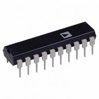
AD670JN Analog Devices Inc, AD670JN Datasheet - Page 7

AD670JN
Manufacturer Part Number
AD670JN
Description
IC ADC 8BIT SGNL COND 20-DIP
Manufacturer
Analog Devices Inc
Datasheet
1.AD670JNZ.pdf
(12 pages)
Specifications of AD670JN
Rohs Status
RoHS non-compliant
Number Of Bits
8
Sampling Rate (per Second)
10k
Data Interface
Parallel
Number Of Converters
1
Power Dissipation (max)
450mW
Voltage Supply Source
Single Supply
Operating Temperature
0°C ~ 70°C
Mounting Type
Through Hole
Package / Case
20-DIP (0.300", 7.62mm)
Available stocks
Company
Part Number
Manufacturer
Quantity
Price
Part Number:
AD670JN
Manufacturer:
ADI/亚德诺
Quantity:
20 000
Company:
Part Number:
AD670JNZ
Manufacturer:
DIODES
Quantity:
12 000
CONTROL AND TIMING OF THE AD670
Control Logic
The AD670 contains on-chip logic to provide conversion and
data read operations from signals commonly available in micro-
processor systems. Figure 7 shows the internal logic circuitry of
the AD670. The control signals, CE, CS, and R/W control the
operation of the converter. The read or write function is deter-
mined by R/W when both CS and CE are low as shown in
Table II. If all three control inputs are held low longer than the
conversion time, the device will continuously convert until one
input, CE, CS, or R/W is brought high. The relative timing of
these signals is discussed later in this section.
REV. A
Boldface indicates parameters tested 100% unless otherwise noted. See Specifications page for explanation.
Figure 6. Transfer Curves
Symbol
WRITE/CONVERT START MODE
t
t
t
t
t
t
READ MODE
t
t
t
t
t
t
6c. Full Scale (Unipolar)
W
DS
DH
RWC
DC
C
R
SD
TD
DH
DT
RT
6b. Bipolar
Parameter
Write/Start Pulse Width
Input Data Setup Time
Input Data Hold
Read/Write Setup Before Control
Delay to Convert Start
Conversion Time
Read Time
Delay from Status Low to Data Read
Bus Access Time
Data Hold Time
Output Float Delay
R/W before CE or CS low
Table III. AD670 TIMING SPECIFICATIONS
–7–
Timing
The AD670 is easily interfaced to a variety of microprocessors
and other digital systems. The following discussion of the timing
requirements of the AD670 control signals will provide the de-
signer with useful insight into the operation of the device.
Write/Convert Start Cycle
Figure 8 shows a complete timing diagram for the write/convert
start cycle. CS (chip select) and CE (chip enable) are active low
and are interchangeable signals. Both CS and CE must be low
for the converter to read or start a conversion. The minimum
pulse width, t
conversion.
300
200
10
0
25
0
Min
250
@ +25 C
R/W
0
1
X
X
Table II. AD670 Control Signal Truth Table
Typ
200
Figure 7. Control Logic Block Diagram
W
, on either CS or CE is 300 ns to start a
CS
0
0
X
1
Max
700
250
250
150
10
CE
0
0
1
X
Units
ns
ns
ns
ns
ns
ns
ns
ns
ns
ns
ns
s
OPERATION
WRITE/CONVERT
READ
NONE
NONE
AD670


