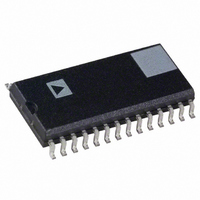
AD9225AR Analog Devices Inc, AD9225AR Datasheet - Page 20

AD9225AR
Manufacturer Part Number
AD9225AR
Description
IC ADC 12BIT 25MSPS 28-SOIC
Manufacturer
Analog Devices Inc
Datasheet
1.AD9225ARZ.pdf
(25 pages)
Specifications of AD9225AR
Mounting Type
Surface Mount
Rohs Status
RoHS non-compliant
Number Of Bits
12
Sampling Rate (per Second)
25M
Data Interface
Parallel
Number Of Converters
7
Power Dissipation (max)
373mW
Voltage Supply Source
Single Supply
Operating Temperature
-40°C ~ 85°C
Package / Case
28-SOIC (0.300", 7.50mm Width)
Power Dissipation Pd
383mW
Input Channels Per Adc
1
No. Of Channels
1
Peak Reflow Compatible (260 C)
No
Sample Rate
25MSPS
Supply Voltage Max
5V
No. Of Bits
12 Bit
For Use With
AD9225-EB - BOARD EVAL FOR AD9225
Lead Free Status / RoHS Status
Contains lead / RoHS non-compliant
Available stocks
Company
Part Number
Manufacturer
Quantity
Price
Part Number:
AD9225AR
Manufacturer:
ADI/亚德诺
Quantity:
20 000
Company:
Part Number:
AD9225ARS
Manufacturer:
ADI
Quantity:
288
Part Number:
AD9225ARS
Manufacturer:
ADI/亚德诺
Quantity:
20 000
Part Number:
AD9225ARSRL
Manufacturer:
ADI/亚德诺
Quantity:
20 000
Company:
Part Number:
AD9225ARSZ
Manufacturer:
ADI
Quantity:
1 000
Part Number:
AD9225ARSZ
Manufacturer:
ADI/亚德诺
Quantity:
20 000
Company:
Part Number:
AD9225ARSZRL
Manufacturer:
ADI
Quantity:
1 000
Part Number:
AD9225ARZ
Manufacturer:
ADI/亚德诺
Quantity:
20 000
AD9225
GROUNDING AND DECOUPLING
Analog and Digital Grounding
Proper grounding is essential in any high speed, high resolution
system. Multilayer printed circuit boards (PCBs) are recom-
mended to provide optimal grounding and power schemes. The
use of ground and power planes offers distinct advantages:
• The minimization of the loop area encompassed by a signal
• The minimization of the impedance associated with ground
• The inherent distributed capacitor formed by the power
These characteristics result in both a reduction of electro-
magnetic interference (EMI) and an overall improvement
in performance.
It is important to design a layout that prevents noise from cou-
pling onto the input signal. Digital signals should not be run in
parallel with input signal traces and should be routed away from
the input circuitry. While the AD9225 features separate analog
and driver ground pins, it should be treated as an analog com-
ponent. The AVSS and DRVSS pins must be joined together
directly under the AD9225. A solid ground plane under the
ADC is acceptable if the power and ground return currents are
Figure 29. IF Undersampling at 70 MHz (F
F
Figure 30. IF Undersampling at 85 MHz (F
F
2
2
and its return path.
and power paths.
plane, PCB insulation and ground plane.
= 70.11 MHz, CLOCK = 25 MHz)
= 85.23 MHz, CLOCK = 20 MHz)
100
95
90
85
80
75
70
65
60
55
50
100
95
90
85
80
75
70
65
60
55
50
–15
–15
DUAL-TONE
DUAL-TONE
(dBFS)
SFDR
(dBFS)
SFDR
–10
–10
SINGLE-TONE
A
A
IN
IN
(dBFS)
SFDR
(dBFS)
(dBFS)
SINGLE-TONE
(dBFS)
SFDR
–5
–5
SINGLE-TONE
SINGLE-TONE
1
(dBc)
1
(dBc)
SNR
SNR
= 69.50 MHz,
= 84.81 MHz,
0
0
–20–
carefully managed. Alternatively, the ground plane under the
ADC may contain serrations to steer currents in predictable
directions where cross coupling between analog and digital
would otherwise be unavoidable. The AD9225/AD9225EB
ground layout, shown in Figure 38, depicts the serrated type
of arrangement.
The board is built primarily over a common ground plane. It
has a slit to route currents near the clock driver. Figure 31 illus-
trates a general scheme of ground and power implementation, in
and around the AD9225.
Analog and Digital Driver Supply Decoupling
The AD9225 features separate analog and driver supply and
ground pins, helping to minimize digital corruption of sensitive
analog signals. In general, AVDD, the analog supply, should
be decoupled to AVSS, the analog common, as close to the
chip as physically possible. Figure 32 shows the recommended
decoupling for the analog supplies; 0.1 mF ceramic chip and
10 mF tantalum capacitors should provide adequately low imped-
ance over a wide frequency range. Note that the AVDD and
AVSS pins are co-located on the AD9225 to simplify the layout
of the decoupling capacitors and provide the shortest possible
PCB trace lengths. The AD9225/AD9225EB power plane layout,
shown in Figure 39 depicts a typical arrangement using a multi-
layer PCB.
The CML is an internal analog bias point used internally by
the AD9225. This pin must be decoupled with at least a 0.1 mF
capacitor as shown in Figure 33. The dc level of CML is
approximately AVDD/2. This voltage should be buffered if it is
to be used for any external biasing.
V
IN
A
D
A
Figure 31. Ground and Power Consideration
= ANALOG
= DIGITAL
Figure 32. Analog Supply Decoupling
ADC
A
IC
10 F
0.1 F
Figure 33. CML Decoupling
CIRCUITS
ANALOG
AVDD
A
A
0.1 F
AVSS
I
A
C
C
STRAY
STRAY
A
CML
CIRCUITS
DIGITAL
AVDD
AVSS
DVDD
A
AD9225
B
DVSS
I
D
AD9225
V
D
DIGITAL
SUPPLY
LOGIC
LOGIC
GND
ICs
Rev. C
D


