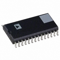
AD9225AR Analog Devices Inc, AD9225AR Datasheet - Page 21

AD9225AR
Manufacturer Part Number
AD9225AR
Description
IC ADC 12BIT 25MSPS 28-SOIC
Manufacturer
Analog Devices Inc
Datasheet
1.AD9225ARZ.pdf
(25 pages)
Specifications of AD9225AR
Mounting Type
Surface Mount
Rohs Status
RoHS non-compliant
Number Of Bits
12
Sampling Rate (per Second)
25M
Data Interface
Parallel
Number Of Converters
7
Power Dissipation (max)
373mW
Voltage Supply Source
Single Supply
Operating Temperature
-40°C ~ 85°C
Package / Case
28-SOIC (0.300", 7.50mm Width)
Power Dissipation Pd
383mW
Input Channels Per Adc
1
No. Of Channels
1
Peak Reflow Compatible (260 C)
No
Sample Rate
25MSPS
Supply Voltage Max
5V
No. Of Bits
12 Bit
For Use With
AD9225-EB - BOARD EVAL FOR AD9225
Lead Free Status / RoHS Status
Contains lead / RoHS non-compliant
Available stocks
Company
Part Number
Manufacturer
Quantity
Price
Part Number:
AD9225AR
Manufacturer:
ADI/亚德诺
Quantity:
20 000
Company:
Part Number:
AD9225ARS
Manufacturer:
ADI
Quantity:
288
Part Number:
AD9225ARS
Manufacturer:
ADI/亚德诺
Quantity:
20 000
Part Number:
AD9225ARSRL
Manufacturer:
ADI/亚德诺
Quantity:
20 000
Company:
Part Number:
AD9225ARSZ
Manufacturer:
ADI
Quantity:
1 000
Part Number:
AD9225ARSZ
Manufacturer:
ADI/亚德诺
Quantity:
20 000
Company:
Part Number:
AD9225ARSZRL
Manufacturer:
ADI
Quantity:
1 000
Part Number:
AD9225ARZ
Manufacturer:
ADI/亚德诺
Quantity:
20 000
Rev. C
The digital activity on the AD9225 chip falls into two general
categories: correction logic and output drivers. The internal
correction logic draws relatively small surges of current, mainly
during the clock transitions. The output drivers draw large
current impulses while the output bits are changing. The size
and duration of these currents are a function of the load on the
output bits; large capacitive loads are to be avoided. Note that
the internal correction logic of the AD9225 is referenced to
AVDD while the output drivers are referenced to DRVDD.
The decoupling shown in Figure 34, a 0.1 mF ceramic chip
capacitor and a 10 mF tantalum capacitor, are appropriate for a
reasonable capacitive load on the digital outputs (typically
20 pF on each pin). Applications involving greater digital loads
should consider increasing the digital decoupling proportionally,
and/or using external buffers/latches.
–21–
A complete decoupling scheme will also include large tantalum
or electrolytic capacitors on the PCB to reduce low frequency
ripple to negligible levels. Refer to the AD9225/AD9225EB
schematic and layouts in Figures 35 to 41 for more information
regarding the placement of decoupling capacitors.
Figure 34. Digital Supply Decoupling
10 F
0.1 F
DRVDD
DRVSS
AD9225
AD9225


