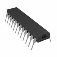
AD7710AN Analog Devices Inc, AD7710AN Datasheet - Page 7

AD7710AN
Manufacturer Part Number
AD7710AN
Description
IC ADC SIGNAL CONDITIONING 24DIP
Manufacturer
Analog Devices Inc
Datasheet
1.AD7710ARZ-REEL.pdf
(32 pages)
Specifications of AD7710AN
Mounting Type
Through Hole
Rohs Status
RoHS non-compliant
Number Of Bits
24
Sampling Rate (per Second)
1.03k
Data Interface
Serial
Number Of Converters
1
Power Dissipation (max)
45mW
Voltage Supply Source
Analog and Digital, Dual ±
Operating Temperature
-40°C ~ 85°C
Package / Case
24-DIP (0.300", 7.62mm)
Peak Reflow Compatible (260 C)
No
No. Of Bits
24 Bit
Leaded Process Compatible
No
Features
24-Bit, Signal Conditioning W/2 Diff. In Ch.
No. Of Channels
2
Interface Type
Serial
Lead Free Status / RoHS Status
Contains lead / RoHS non-compliant
Available stocks
Company
Part Number
Manufacturer
Quantity
Price
Part Number:
AD7710ANZ
Manufacturer:
ADI/亚德诺
Quantity:
20 000
REV. G
Pin Mnemonic
1
2
3
4
5
6
7
8
9
10
11
12
13
14
15
16
17
18
SCLK
MCLK IN
MCLK OUT When the master clock for the device is a crystal, the crystal is connected between MCLK IN and MCLK OUT.
A0
SYNC
MODE
AIN1(+)
AIN1(–)
AIN2(+)
AIN2(–)
V
AV
V
REF IN(–)
REF IN(+)
REF OUT
I
AGND
OUT
SS
BIAS
DD
Function
Serial Clock. Logic input/output, depending on the status of the MODE pin. When MODE is high, the
device is in its self-clocking mode, and the SCLK pin provides a serial clock output. This SCLK becomes
active when RFS or TFS goes low, and it goes high impedance when either RFS or TFS returns high or when
the device has completed transmission of an output word. When MODE is low, the device is in its external
clocking mode, and the SCLK pin acts as an input. This input serial clock can be a continuous clock with all
data transmitted in a continuous train of pulses. Alternatively, it can be a noncontinuous clock with the
information being transmitted to the AD7710 in smaller batches of data.
Master Clock Signal for the Device. This can be provided in the form of a crystal or external clock. A crystal
can be tied across the MCLK IN and MCLK OUT pins. Alternatively, the MCLK IN pin can be driven with
a CMOS compatible clock and MCLK OUT left unconnected. The clock input frequency is nominally 10 MHz.
Address Input. With this input low, reading and writing to the device is to the control register. With this
input high, access is to either the data register or the calibration registers.
Logic Input. Allows for synchronization of the digital filters when using a number of AD7710s. It resets
the nodes of the digital filter.
Logic Input. When this pin is high, the device is in its self-clocking mode; with this pin low, the device is in
its external clocking mode.
Analog Input Channel 1. Positive input of the programmable gain differential analog input. The AIN1(+)
input is connected to an output current source that can be used to check that an external transducer has
burned out or gone open circuit. This output current source can be turned on/off via the control register.
Analog Input Channel 1. Negative input of the programmable gain differential analog input.
Analog Input Channel 2. Positive input of the programmable gain differential analog input.
Analog Input Channel 2. Negative input of the programmable gain differential analog input.
Analog Negative Supply, 0 V to –5 V. Tied to AGND for single-supply operation. The input voltage on
AIN1 or AIN2 should not go > 30 mV negative w.r.t. V
Analog Positive Supply Voltage, 5 V to 10 V.
Input Bias Voltage. This input voltage should be set such that V
0.85
AV
and V
Reference Input. The REF IN(–) can lie anywhere between AV
than REF IN(–).
Reference Input. The reference input is differential providing that REF IN(+) is greater than REF IN(–).
REF IN(+) can lie anywhere between AV
Reference Output. The internal 2.5 V reference is provided at this pin. This is a single-ended output which
is referred to AGND. It is a buffered output which is capable of providing 1 mA to an external load.
Compensation Current Output. A 20 A constant current is provided at this pin. This current can be used in
association with an external thermistor to provide cold junction compensation in thermocouple applications.
This current can be turned on or off via the control register.
Ground Reference Point for Analog Circuitry.
DD
SS
and V
V
= –5 V, it can be tied to AGND; with AV
REF
> V
SS
. Thus with AV
SS
where V
PIN FUNCTION DESCRIPTIONS
REF
DD
is REF IN(+) – REF IN(–). Ideally, this should be tied halfway between
= 5 V and V
DD
–7–
and V
SS
= 0 V, it can be tied to REF OUT; with AV
DD
SS
.
= 10 V, it can be tied to 5 V.
SS
for correct operation of the device.
DD
BIAS
and V
+ 0.85
SS
provided REF IN(+) is greater
V
REF
< AV
DD
and V
DD
= 5 V
AD7710
BIAS
–


