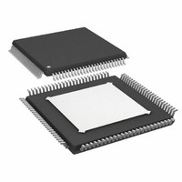
AD9271BSVZ-25 Analog Devices Inc, AD9271BSVZ-25 Datasheet - Page 27

AD9271BSVZ-25
Manufacturer Part Number
AD9271BSVZ-25
Description
IC ADC OCT 12BIT 25MSPS 100-TQFP
Manufacturer
Analog Devices Inc
Datasheet
1.AD9271BSVZ-50.pdf
(60 pages)
Specifications of AD9271BSVZ-25
Data Interface
Serial, SPI™
Number Of Bits
12
Sampling Rate (per Second)
25M
Number Of Converters
8
Power Dissipation (max)
1.06W
Voltage Supply Source
Single Supply
Operating Temperature
-40°C ~ 85°C
Mounting Type
Surface Mount
Package / Case
100-TQFP Exposed Pad
Resolution (bits)
12bit
Sampling Rate
50MSPS
Input Channel Type
Differential, Single Ended
Supply Voltage Range - Digital
1.7V To 1.9V
Supply Current
505mA
Lead Free Status / RoHS Status
Lead free / RoHS Compliant
For Use With
AD9271-50EBZ - BOARD EVALUATION AD9271 50MSPS
Lead Free Status / RoHS Status
Lead free / RoHS Compliant, Lead free / RoHS Compliant
Available stocks
Company
Part Number
Manufacturer
Quantity
Price
Company:
Part Number:
AD9271BSVZ-25
Manufacturer:
AD
Quantity:
1 600
Company:
Part Number:
AD9271BSVZ-25
Manufacturer:
Analog Devices Inc
Quantity:
10 000
noise voltage is simply equal to the output noise divided by the
measured gain at each point in the control range.
The output-referred noise is a flat 63 nV/√Hz over most of the
gain range, because it is dominated by the fixed output-referred
noise of the VGA. At the high end of the gain control range, the
noise of the LNA and source prevail. The input-referred noise
reaches its minimum value near the maximum gain control
voltage, where the input-referred contribution of the VGA is
miniscule.
At lower gains, the input-referred noise and, therefore, the noise
figure increases as the gain decreases. The instantaneous dynamic
range of the system is not lost, however, because the input capacity
increases as the input-referred noise increases. The contribution
of the ADC noise floor has the same dependence. The important
relationship is the magnitude of the VGA output noise floor
relative to that of the ADC.
Gain control noise is a concern in very low noise applications.
Thermal noise in the gain control interface can modulate the
channel gain. The resultant noise is proportional to the output
signal level and is usually evident only when a large signal is
present. The gain interface includes an on-chip noise filter, which
significantly reduces this effect at frequencies above 5 MHz. Care
should be taken to minimize noise impinging at the GAIN±
input. An external RC filter can be used to remove V
noise. The filter bandwidth should be sufficient to accommodate
the desired control bandwidth.
Antialiasing Filter
The filter that the signal reaches prior to the ADC is used to
reject dc signals and to band limit the signal for antialiasing.
Figure 53 shows the architecture of the filter.
*C = 0.5pF TO 3.1pF
56pF/112pF
56pF/112pF
Figure 53. Simplified Filter Schematic
2kΩ
2kΩ
7.5C*
2kΩ
2kΩ
6.5C*
2kΩ
2kΩ
4kΩ
4kΩ
1C*
1C*
GAIN
source
Rev. B | Page 27 of 60
The filter can be configured for dc coupling or to have a single
pole for high-pass filtering at either 700 kHz or 350 kHz
(programmed through the SPI). The high-pass pole, however, is
not tuned and can vary by ±30%.
A third-order Butterworth low-pass filter is used to reduce
noise bandwidth and provide antialiasing for the ADC. The
filter uses on-chip tuning to trim the capacitors and in turn set
the desired cutoff frequency and reduce variations. The default
−3 dB cutoff is 1/3 the ADC sample clock rate. The cutoff can
be scaled to 0.7, 0.8, 0.9, 1, 1.1, 1.2, or 1.3 times this frequency
through the SPI. The cutoff can be set from 8 MHz to 18 MHz.
Tuning is normally off to avoid changing the capacitor settings
during critical times. The tuning circuit is enabled and disabled
through the SPI. Initializing the tuning of the filter must be
done after initial power-up and after reprogramming the filter
cutoff scaling or ADC sample rate. Occasional retuning during
an idle time is recommended to compensate for temperature drift.
ADC
The AD9271 architecture consists of a pipelined ADC divided
into three sections: a 4-bit first stage followed by eight 1.5-bit
stages and a 3-bit flash. Each stage provides sufficient overlap to
correct for flash errors in the preceding stages. The quantized
outputs from each stage are combined into a 12-bit result in the
digital correction logic. The pipelined architecture permits the
first stage to operate on a new input sample and the remaining
stages to operate on preceding samples. Sampling occurs on the
rising edge of the clock.
Each stage of the pipeline except for the last consists of a low
resolution flash ADC connected to a switched-capacitor DAC
and interstage residue amplifier (for example, a multiplying
digital-to-analog converter (MDAC)). The residue amplifier
magnifies the difference between the reconstructed DAC output
and the flash input for the next stage in the pipeline. One bit of
redundancy is used in each stage to facilitate digital correction
of flash errors. The last stage consists of a flash ADC.
The output staging block aligns the data, carries out error cor-
rection, and passes the data to the output buffers. The data is
then serialized and aligned to the frame and output clock.
AD9271


