AD7870SQ Analog Devices Inc, AD7870SQ Datasheet - Page 22
AD7870SQ
Manufacturer Part Number
AD7870SQ
Description
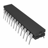
IC ADC 12BIT SAMPLING 3V 24-CDIP
Manufacturer
Analog Devices Inc
Datasheet
1.AD7870JNZ.pdf
(28 pages)
Specifications of AD7870SQ
Rohs Status
RoHS non-compliant
Number Of Bits
12
Sampling Rate (per Second)
100k
Data Interface
Serial, Parallel
Number Of Converters
1
Power Dissipation (max)
95mW
Voltage Supply Source
Dual ±
Operating Temperature
-55°C ~ 125°C
Mounting Type
Through Hole
Package / Case
24-CDIP (0.300", 7.62mm)
Available stocks
Company
Part Number
Manufacturer
Quantity
Price
Company:

Part Number:
AD7870SQ/883B
Manufacturer:
NEC
Quantity:
41


AD7870/AD7875/AD7876
APPLICATIONS INFORMATION
Good printed circuit board (PCB) layout is as important as
the overall circuit design itself in achieving high speed analog-
to-digital performance. The designer has to be conscious of
noise both in the ADC itself and in the preceding analog
circuitry. Switching mode power supplies are not recommended
because the switching spikes feed through to the comparator
causing noisy code transitions. Other causes of concern are
ground loops and digital feedthrough from microprocessors.
These are factors which influence any ADC, and a proper
PCB layout which minimizes these effects is essential for best
performance.
LAYOUT HINTS
Ensure that the layout for the printed circuit board has the
digital and analog signal lines separated as much as possible.
Take care not to run any digital track alongside an analog signal
track. Guard (screen) the analog input with AGND.
Establish a single point analog ground (star ground) separate
from the logic system ground at the AGND pin or as close
as possible to the ADC. Connect all other grounds and the
Rev. C | Page 22 of 28
AD7870/AD7875/AD7876 DGND to this single analog
ground point. Do not connect any other digital grounds to
this analog ground point.
Low impedance analog and digital power supply common
returns are essential to low noise operation of the ADC, so
make the foil width for these tracks as wide as possible. The
use of ground planes minimizes impedance paths and also
guards the analog circuitry from digital noise. The circuit
layout has both analog and digital ground planes which are
kept separated and only joined together at the AD7870/
AD7875/AD7876 AGND pin.
NOISE
Keep the input signal leads to V
AGND as short as possible to minimize input noise coupling.
In applications where this is not possible, use a shielded cable
between the source and the ADC. Reduce the ground circuit
impedance as much as possible since any potential difference
in grounds between the signal source and the ADC appears as
an error voltage in series with the input signal.
IN
and signal return leads from
Related parts for AD7870SQ
Image
Part Number
Description
Manufacturer
Datasheet
Request
R

Part Number:
Description:
±1.7g Dual-Axis IMEMS Accelerometer Evaluation Board
Manufacturer:
Analog Devices Inc
Datasheet:

Part Number:
Description:
Inertial Sensor Evaluation System
Manufacturer:
Analog Devices Inc
Datasheet:
Part Number:
Description:
Manufacturer:
Analog Devices Inc
Datasheet:
Part Number:
Description:
Manufacturer:
Analog Devices Inc
Datasheet:
Part Number:
Description:
Manufacturer:
Analog Devices Inc
Datasheet:
Part Number:
Description:
Manufacturer:
Analog Devices Inc
Datasheet:
Part Number:
Description:
Manufacturer:
Analog Devices Inc
Datasheet:
Part Number:
Description:
Manufacturer:
Analog Devices Inc
Datasheet:
Part Number:
Description:
Manufacturer:
Analog Devices Inc
Datasheet:
Part Number:
Description:
Manufacturer:
Analog Devices Inc
Datasheet:
Part Number:
Description:
Manufacturer:
Analog Devices Inc
Datasheet:
Part Number:
Description:
Manufacturer:
Analog Devices Inc
Datasheet:
Part Number:
Description:
Manufacturer:
Analog Devices Inc
Datasheet: