ADADC80-12 Analog Devices Inc, ADADC80-12 Datasheet - Page 10
ADADC80-12
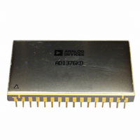
Manufacturer Part Number
ADADC80-12
Description
IC ADC 12-BIT INTEGRATED 32-CDIP
Manufacturer
Analog Devices Inc
Datasheet
1.ADADC80-12.pdf
(16 pages)
Specifications of ADADC80-12
Data Interface
Parallel
Rohs Status
RoHS non-compliant
Number Of Bits
12
Sampling Rate (per Second)
40k
Number Of Converters
1
Power Dissipation (max)
800mW
Voltage Supply Source
Analog and Digital, Dual ±
Operating Temperature
-25°C ~ 85°C
Mounting Type
Through Hole
Package / Case
32-CDIP (0.900", 22.86mm)
Resolution (bits)
12bit
Input Channel Type
Single Ended
Supply Current
70mA
Digital Ic Case Style
DIP
No. Of Pins
32
Operating Temperature Range
-25°C To +85°C
Number Of Elements
1
Resolution
12Bit
Architecture
SAR
Input Polarity
Unipolar/Bipolar
Input Type
Voltage
Rated Input Volt
5/10/±2.5/±5/±10V
Differential Input
No
Power Supply Requirement
Dual
Single Supply Voltage (typ)
Not RequiredV
Single Supply Voltage (min)
Not RequiredV
Single Supply Voltage (max)
Not RequiredV
Dual Supply Voltage (typ)
±15/5V
Dual Supply Voltage (min)
±14/4.75V
Dual Supply Voltage (max)
±16/5.25V
Differential Linearity Error
±0.5LSB(Typ)
Integral Nonlinearity Error
±0.012%FSR
Operating Temp Range
-25C to 85C
Operating Temperature Classification
Commercial
Mounting
Through Hole
Pin Count
32
Package Type
SBCDIP
Input Signal Type
Single-Ended
Lead Free Status / Rohs Status
Not Compliant
Available stocks
Company
Part Number
Manufacturer
Quantity
Price

Part Number:
ADADC80-12
Manufacturer:
AD
Quantity:
20 000


ADADC80
Table 6. Input Voltage Range and LSB Values
Binary Output
Analog Input Voltage Range
Code Designation
One Least Significant Bit (LSB)
Transition Values
MSB LSB
000. . . 000
011. . . 111
111. . . 110
1
2
3
4
OFFSET ADJUSTMENT
The zero adjust circuit consists of a potentiometer connected
across ±V
to COMPARATOR IN (Pin 11) for all ranges. As shown in
Figure 9, the tolerance of this fixed resistor is not critical, and a
carbon composition type is generally adequate. Using a carbon
composition resistor with a −1200 ppm/°C tempco contributes
a worst-case offset tempco of 8 × 244 × 10
2.3 ppm/°C of FSR if the offset adjustment potentiometer is set
at either end of its adjustment range. Because the maximum
offset adjustment required is typically no more than ±4 LSB,
use of a carbon composition offset summing resistor typically
contributes no more than 1 ppm/°C of FSR offset tempco.
An alternative offset adjust circuit, which contributes negligible
offset tempco if metal film resistors (tempco < 100 ppm/°C) are
used, is shown in Figure 10. Note that the abbreviation MF in
Figure 10 and Figure 12 refer to metal film resistors.
COB = complementary offset binary.
CTC = complementary twos complement; obtained by using the complement of the most significant bit ( MSB ). MSB is available on Pin 8.
CSB = complementary straight binary.
Voltages given are the nominal value for transition to the code specified.
OFFSET
ADJUST
S
4
with its slider connected through a 1.8 MΩ resistor
Figure 10. Low Tempco Zero Adjustment Circuit
100kΩ
100kΩ
10kΩ
10kΩ
TO
TO
+15V
–15V
+15V
–15V
Figure 9. Offset Adjustment Circuit
COMPARATOR
180kΩ
MF
22kΩ
1.8MΩ
MF
COMPARATOR
A
IN
11
180kΩ
Defined as
FSR
2
n = 8
n = 10
n = 12
+Full scale
Midscale
−Full scale
MF
ADADC80
n
IN
11
−6
× 1200 ppm/°C =
ADADC80
±10 V
COB
or CTC
20 V
2
78.13 mV
19.53 mV
4.88 mV
10 V − 3/2 LSB
0
−10 V + 1/2 LSB
n
1
2
Rev. E | Page 10 of 16
±5 V
COB
or CTC
10 V
2
39.06 mV
9.77 mV
2.44 mV
5 V − 3/2 LSB
0
−5 V + 1/2 LSB
n
In either zero adjust circuit, the fixed resistor connected to
COMPARATOR IN (Pin 11) should be located close to this pin
to keep the pin connection runs short. Pin 11 is quite sensitive
to external noise pickup.
GAIN ADJUSTMENT
The gain adjust circuit consists of a potentiometer connected
across ±V
to the GAIN ADJUST (Pin 16), as shown in Figure 11.
An alternative gain adjust circuit, which contributes negligible
gain tempco if metal film resistors (tempco < 100 ppm/°C) are
used, is shown in Figure 12.
1
2
ADJUST
100kΩ
GAIN
10kΩ
S
with its slider connected through a 10 MΩ resistor
TO
Figure 12. Low Tempco Gain Adjustment Circuit
+15V
–15V
±2.5 V
COB
or CTC
5 V
2
2.5 V − 3/2 LSB
−2.5 V + 1/2 LSB
19.53 mV
4.88 mV
1.22 mV
0
100kΩ
n
10kΩ
TO
270kΩ
Figure 11. Gain Adjustment Circuit
+15V
–15V
6.8kΩ
1
MF
2
10MΩ
270kΩ
0.1µF
MF
ADJUST
0.01µF
0 V to +10 V
CSB
10 V
2
39.06 mV
9.77 mV
2.44 mV
10 V − 3/2 LSB
5 V
0 V + 1/2 LSB
ADJUST
n
GAIN
GAIN
3
16
16
ADADC80
ADADC80
0 V to +5 V
CSB
5 V
2
19.53 mV
4.88 mV
1.22 mV
5 V − 3/2 LSB
2.5 V
0 V + 1/2 LSB
n
3
Related parts for ADADC80-12
Image
Part Number
Description
Manufacturer
Datasheet
Request
R

Part Number:
Description:
IC ADC 12BIT INTEGRATED 32-CDIP
Manufacturer:
Analog Devices Inc
Datasheet:

Part Number:
Description:
±1.7g Dual-Axis IMEMS Accelerometer Evaluation Board
Manufacturer:
Analog Devices Inc
Datasheet:

Part Number:
Description:
Inertial Sensor Evaluation System
Manufacturer:
Analog Devices Inc
Datasheet:
Part Number:
Description:
Manufacturer:
Analog Devices Inc
Datasheet:
Part Number:
Description:
Manufacturer:
Analog Devices Inc
Datasheet:
Part Number:
Description:
Manufacturer:
Analog Devices Inc
Datasheet:
Part Number:
Description:
Manufacturer:
Analog Devices Inc
Datasheet:
Part Number:
Description:
Manufacturer:
Analog Devices Inc
Datasheet:
Part Number:
Description:
Manufacturer:
Analog Devices Inc
Datasheet:
Part Number:
Description:
Manufacturer:
Analog Devices Inc
Datasheet:
Part Number:
Description:
Manufacturer:
Analog Devices Inc
Datasheet:
Part Number:
Description:
Manufacturer:
Analog Devices Inc
Datasheet:
Part Number:
Description:
Manufacturer:
Analog Devices Inc
Datasheet: