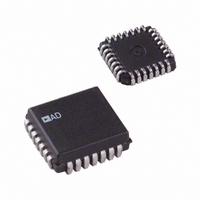
AD1555BP Analog Devices Inc, AD1555BP Datasheet - Page 16

AD1555BP
Manufacturer Part Number
AD1555BP
Description
IC ADC PGA 24BIT LN 28PLCC
Manufacturer
Analog Devices Inc
Datasheet
1.AD1555APZ.pdf
(24 pages)
Specifications of AD1555BP
Rohs Status
RoHS non-compliant
Number Of Bits
24
Sampling Rate (per Second)
256k
Data Interface
Serial, Parallel
Number Of Converters
1
Power Dissipation (max)
96W
Voltage Supply Source
Dual ±
Operating Temperature
-55°C ~ 85°C
Mounting Type
Surface Mount
Package / Case
28-LCC (J-Lead)
For Use With
EVAL-AD1555/56EB - BOARD EVAL FOR AD1555/56
Available stocks
Company
Part Number
Manufacturer
Quantity
Price
Company:
Part Number:
AD1555BPRL
Manufacturer:
Analog Devices Inc
Quantity:
10 000
Company:
Part Number:
AD1555BPZ
Manufacturer:
Analog Devices Inc
Quantity:
10 000
Company:
Part Number:
AD1555BPZRL
Manufacturer:
Analog Devices Inc
Quantity:
10 000
CIRCUIT DESCRIPTION
The AD1555/AD1556 chipset is a complete sigma-delta 24-bit
A/D converter with very high dynamic range intended for the
measurement of low frequency signals up to a few kHz such as
those in seismic applications.
The AD1555 contains an analog multiplexer, a fully differential
programmable gain amplifier and a fourth order sigma-delta
modulator. The analog multiplexer allows selection of one fully
differential input from two different external inputs, an internal
ground reference or an internal full-scale voltage reference. The
fully differential programmable gain amplifier (PGA) has five gain
settings of 1, 2.5, 8.5, 34, and 128, which allow the part to handle
a total of five different input ranges: 1.6 V rms, 636 mV rms,
187 mV rms, 47 mV rms, and 12.4 mV rms that are programmed
via digital input pins (CB0 to CB4). The modulator that operates
nominally at a sampling frequency of 256 kHz, outputs a bit-
stream whose ones-density is proportional to its input voltage.
This bitstream can be filtered using the AD1556, which is a
digital finite impulse low pass filter (FIR). The AD1556 outputs
the data in a 24-bit word over a serial interface. The cutoff
frequency and output rate of this filter can be programmed via
an on-chip register or by hardware through digital input pins.
The dynamic performance and the equivalent input noise vary
with gain and output rate as shown in Table I. The use of the
different PGA gain settings allows enhancement of the total system
dynamic range up to 146 dB (gain of 34 or 128 and F
AD1555/AD1556
HYDROPHONE...
GEOPHONE,
SENSOR:
+5V
100nF
15
SOURCE
3
AC SINE
T
T
TO OTHER AD1555s
TEST
R1
R2
1
2
+5V
ADG609
9
DB DA
C
C
R3
R4
DC TEST
SOURCE
1
2
8
C3
10 F
7
8
5
6
3, 26
15
14
TIN (+)
TIN (–)
AIN (+)
AIN (–)
PGAOUT MODIN REFIN REFCAP1 AGND3
+V
100nF
A
2
100nF
–5V
Figure 7. Typical Operating Circuit
AGND1
1
O
28
AD1555
= 250 Hz).
AGND2
27
100nF
25
–V
6
3
A
TEM
P
4, 20, 21
V
–16–
23
OUT
22 F
CB0...CB4
AD780
MDATA
GND
The AD1555 operates from a dual analog supply (± 5 V),
while the digital part of the AD1555 operates from a +5 V
supply. The AD1556 operates from a single 3.3 V or 5 V
supply. Each device exhibits low power dissipation and can
be configured for standby mode.
Figure 7 illustrates a typical operating circuit.
MULTIPLEXER AND PROGRAMMABLE GAIN
AMPLIFIER (PGA)
Analog Inputs
The AD1555 has two sets of fully differential inputs AIN and
TIN. The common-mode rejection capability of these inputs
generally surpasses the performance of conventional program-
mable gain amplifiers. The very high input impedance, typically
higher than 140 MΩ, allows direct connection of the sensor to
the AD1555 inputs, even through serial resistances. Figure 7
illustrates such a configuration. The passive filter between the
sensor and the AD1555 is shown here as an example. Other
filter structures could be used, depending on the specific require-
ments of the application. Also, the Johnson noise (√4 k TRB) of
the serial resistance should be taken into consideration. For
instance, a 1 kΩ serial resistance reduces by approximately 1.3 dB
the dynamic performance of a system using a gain setting of
128 at an output word rate F
where the sensor inputs must be protected against severe
10 F
MFLG
MCLK
DGND
4
22
V
–5V
L
O/P
100nF
+V
15
17
18
19
16
IN
8
2
5
+5V
100nF
15
10 F
+5V
V
DIG
11, 22, 44
MCLK
CB0...CB4
MFLG
MDATA
UNUSED AD1555 PINS MUST BE LEFT
UNCONNECTED;
UNUSED AD1556 INPUT PINS MUST BE
TIED TO DGND OR V
CLOCK SOURCE
1.024MHz
AD1556
V
L
100nF
O
32
RESETD
ERROR
TDATA
RESET
= 500 Hz. For applications
DGND
DOUT
DRDY
SCLK
SYNC
RSEL
R/W
DIN
H/S
CS
12, 23, 24, 34
L
16
17
18
30
13
19
14
15
20
31
25
10
37
.
ADSP-21xxx OR P
TO OTHER AD1556s
HARDWARE
SERIAL DATA
CONTROL
INTERFACE
REV. B


