KAD2708C-27Q68 Intersil, KAD2708C-27Q68 Datasheet - Page 3
KAD2708C-27Q68
Manufacturer Part Number
KAD2708C-27Q68
Description
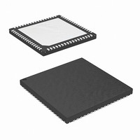
IC ADC 8BIT 275MSPS PAR 68-QFN
Manufacturer
Intersil
Series
FemtoCharge™r
Datasheet
1.KAD2708C-10Q68.pdf
(16 pages)
Specifications of KAD2708C-27Q68
Number Of Bits
8
Sampling Rate (per Second)
275M
Data Interface
Parallel
Number Of Converters
1
Power Dissipation (max)
294mW
Voltage Supply Source
Single Supply
Operating Temperature
-40°C ~ 85°C
Mounting Type
Surface Mount
Package / Case
68-VQFN Exposed Pad, 68-HVQFN, 68-SQFN, 68-DHVQFN
For Use With
KDC2708CEVAL - DAUGHTER CARD FOR KAD2708
Lead Free Status / RoHS Status
Lead free / RoHS Compliant


Electrical Specifications
DC SPECIFICATIONS
Analog Input
Full-Scale Analog
Input Range
Full Scale Range
Temp. Drift
Common-Mode
Output Voltage
Power Requirements
1.8V Analog
Supply Voltage
3.3V Analog
Supply Voltage
1.8V Digital
Supply Voltage
1.8V Analog
Supply Current
3.3V Analog
Supply Current
1.8V Digital
Supply Current
Power
Dissipation
AC SPECIFICATIONS
Maximum
Conversion Rate
PARAMETER
Absolute Maximum Ratings
AVDD2 to AVSS. . . . . . . . . . . . . . . . . . . . . . . . . . . . . . -0.4V to 2.1V
AVDD3 to AVSS. . . . . . . . . . . . . . . . . . . . . . . . . . . . . . -0.4V to 3.7V
OVDD2 to OVSS . . . . . . . . . . . . . . . . . . . . . . . . . . . . . -0.4V to 2.1V
Analog Inputs to AVSS. . . . . . . . . . . . . . . . . -0.4V to AVDD3 + 0.3V
Clock Inputs to AVSS. . . . . . . . . . . . . . . . . . -0.4V to AVDD2 + 0.3V
Logic Inputs to AVSS (VREFSEL, CLKDIV) -0.4V to AVDD3 + 0.3V
Logic Inputs to OVSS (RST, 2SC) . . . . . . . . -0.4V to OVDD2 + 0.3V
VREF to AVSS . . . . . . . . . . . . . . . . . . . . . . . -0.4V to AVDD3 + 0.3V
Analog Output Currents . . . . . . . . . . . . . . . . . . . . . . . . . . . . . . 10mA
Logic Output Currents . . . . . . . . . . . . . . . . . . . . . . . . . . . . . . . 10mA
CMOS Output Currents . . . . . . . . . . . . . . . . . . . . . . . . . . . . . . 20mA
CAUTION: Do not operate at or near the maximum ratings listed for extended periods of time. Exposure to such conditions may adversely impact product reliability and
result in failures not covered by warranty.
NOTES:
3. θ
4. For θ
Tech Brief TB379.
JA
is measured in free air with the component mounted on a high effective thermal conductivity test board with “direct attach” features. See
JC
, the “case temp” location is the center of the exposed metal pad on the package underside.
SYMBOL CONDITIONS
AVDD2
AVDD3
I
I
f
OVDD
I
S
AVDD2
AVDD3
A
OVDD
V
V
P
VTC
MAX
CM
FS
D
Full Temp
All specifications apply under the following conditions unless otherwise noted: AVDD2 = 1.8V, AVDD3 = 3.3V,
OVDD = 1.8V, T
105MSPS, f
+85°C.
3
IN
(Note 5)
= Nyquist at -0.5dBFS. Boldface limits apply over the operating temperature range, -40°C to
MIN
3.15
275
1.4
1.7
1.7
A
= -40°C to +85°C (typical specifications at +25°C), f
KAD2708C-27
TYP
230
860
261
1.5
1.8
3.3
1.8
44
41
26
(Note 5)
MAX
3.45
294
1.6
1.9
1.9
51
45
30
KAD2708C
(Note 5)
3.15
MIN
210
1.4
1.7
1.7
KAD2708C-21
TYP
210
860
222
1.5
1.8
3.3
1.8
Thermal Information
Thermal Resistance (Typical, Notes 3, 4) θ
Operating Temperature . . . . . . . . . . . . . . . . . . . . . . .-40°C to +85°C
Storage Temperature . . . . . . . . . . . . . . . . . . . . . . . .-65°C to +150°C
Junction Temperature . . . . . . . . . . . . . . . . . . . . . . . . . . . . . . +150°C
38
33
25
68 Ld QFN Package. . . . . . . . . . . . . . .
(Note 5)
MAX
3.45
248
1.6
1.9
1.9
42
37
28
(Note 5)
3.15
MIN
170
1.4
1.7
1.7
KAD2708C-17
SAMPLE
TYP
198
860
199
1.5
1.8
3.3
1.8
35
28
24
= 275MSPS, 210MSPS, 170MSPS and
(Note 5)
MAX
3.45
224
1.6
1.9
1.9
39
32
27
(Note 5)
3.15
MIN
105
1.4
1.7
1.7
KAD2708C-10
JA
(°C/W)
23
TYP
178
860
163
1.5
1.8
3.3
1.8
29
21
23
(Note 5)
θ
MAX
3.45
April 14, 2011
185
JC
1.6
1.9
1.9
33
24
26
FN6812.1
1.8
(°C/W)
ppm/°C
UNITS
MSPS
V
mW
mV
mA
mA
mA
P-P
V
V
V
Related parts for KAD2708C-27Q68
Image
Part Number
Description
Manufacturer
Datasheet
Request
R

Part Number:
Description:
IC ADC 8BIT 170MSPS SGL 68-QFN
Manufacturer:
Intersil
Datasheet:

Part Number:
Description:
IC ADC 8BIT 105MSPS SGL 68-QFN
Manufacturer:
Intersil
Datasheet:
Part Number:
Description:
IC ADC 8BIT 210MSPS SGL 68-QFN
Manufacturer:
Intersil
Datasheet:

Part Number:
Description:
Intersil Corporation [CMOS Serial Controller Interface]
Manufacturer:
Intersil Corporation
Datasheet:
Part Number:
Description:
Manufacturer:
Intersil Corporation
Datasheet:
Part Number:
Description:
357-036-542-201 CARDEDGE 36POS DL .156 BLK LOPRO
Manufacturer:
Intersil Corporation
Datasheet:
Part Number:
Description:
1024-Word x 4-Bit LSI Static RAM
Manufacturer:
Intersil Corporation
Datasheet:
Part Number:
Description:
General Purpose NPN Transistor Arrays FN341.4
Manufacturer:
Intersil Corporation
Datasheet:
Part Number:
Description:
CMOS 16-Bit Microprocessor
Manufacturer:
Intersil Corporation
Datasheet:
Part Number:
Description:
Manufacturer:
Intersil Corporation
Datasheet:
Part Number:
Description:
Manufacturer:
Intersil Corporation
Datasheet:
Part Number:
Description:
Manufacturer:
Intersil Corporation
Datasheet:
Part Number:
Description:
Manufacturer:
Intersil Corporation
Datasheet:
Part Number:
Description:
CMOS 6-Bit Latch and Decoder Memory Interfaces
Manufacturer:
Intersil Corporation
Datasheet:
Part Number:
Description:
CA3046General Purpose NPN Transistor Arrays
Manufacturer:
Intersil Corporation
Datasheet: