KAD2710C-17Q68 Intersil, KAD2710C-17Q68 Datasheet - Page 15
KAD2710C-17Q68
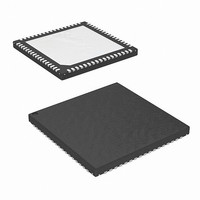
Manufacturer Part Number
KAD2710C-17Q68
Description
IC ADC 10BIT 170MSPS SGL 68-QFN
Manufacturer
Intersil
Series
FemtoCharge™r
Datasheet
1.KAD2710C-10Q68.pdf
(16 pages)
Specifications of KAD2710C-17Q68
Number Of Bits
10
Sampling Rate (per Second)
170M
Data Interface
Parallel
Number Of Converters
1
Power Dissipation (max)
224mW
Voltage Supply Source
Single Supply
Operating Temperature
-40°C ~ 85°C
Mounting Type
Surface Mount
Package / Case
68-VQFN Exposed Pad, 68-HVQFN, 68-SQFN, 68-DHVQFN
For Use With
KDC2710CEVAL - DAUGHTER CARD FOR KAD2710
Lead Free Status / RoHS Status
Lead free / RoHS Compliant


Layout Considerations
Split Ground and Power Planes
Data converters operating at high sampling frequencies
require extra care in PC board layout. If analog and digital
ground planes are separate, analog supply and ground
planes should be laid out under signal and clock inputs and
digital planes under outputs and logic pins. Grounds should
be joined under the chip.
Clock Input Considerations
Use matched transmission lines to the inputs for the analog
input and clock signals. Locate transformers, drivers and
terminations as close to the chip as possible.
Bypass and Filtering
Bulk capacitors should have low equivalent series
resistance. Tantalum is recommended. Keep ceramic
bypass capacitors very close to device pins. Longer traces
will increase inductance, resulting in diminished dynamic
performance and accuracy. Make sure that connections to
ground are direct, and low impedance.
LVCMOS Outputs
Output traces and connections must be designed for 50Ω
characteristic impedance. Keep trace lengths equal, and
minimize bends where possible. Avoid crossing ground and
power-plane breaks with signal traces.
Unused Inputs
The RST and 2SC inputs are internally pulled up, and can be
left open-circuit if not used.
CLKDIV is internally pulled low, which divides the input clock
by two.
VREFSEL must be held low for internal reference, but can
be left open for external reference.
Definitions
Analog Input Bandwidth is the analog input frequency at
which the spectral output power at the fundamental
frequency (as determined by FFT analysis) is reduced by
3dB from its full-scale low-frequency value. This is also
referred to as Full Power Bandwidth.
Aperture Delay or Sampling Delay is the time required
after the rise of the clock input for the sampling switch to
open, at which time the signal is held for conversion.
Aperture Jitter is the RMS variation in aperture delay for a
set of samples.
Clock Duty Cycle is the ratio of the time the clock wave is at
logic high to the total time of one clock period.
Differential Non-Linearity (DNL) is the deviation of any
code width from an ideal 1 LSB step.
15
KAD2710C
Effective Number of Bits (ENOB) is an alternate method of
specifying Signal to Noise-and-Distortion Ratio (SINAD). In
dB, it is calculated as: ENOB = (SINAD - 1.76)/6.02
Gain Error is the ratio of the difference between the voltages
that cause the lowest and highest code transitions to the
full-scale voltage (less 2 LSB). It is typically expressed in
percent.
Integral Non-Linearity (INL) is the deviation of each
individual code from a line drawn from negative full-scale
(1/2 LSB below the first code transition) through positive
full-scale (1/2 LSB above the last code transition). The
deviation of any given code from this line is measured from
the center of that code.
Least Significant Bit (LSB) is the bit that has the smallest
value or weight in a digital word. Its value in terms of input
voltage is V
Missing Codes are output codes that are skipped and will
never appear at the ADC output. These codes cannot be
reached with any input value.
Most Significant Bit (MSB) is the bit that has the largest
value or weight.
Pipeline Delay is the number of clock cycles between the
initiation of a conversion and the appearance at the output
pins of the data.
Power Supply Rejection Ratio (PSRR) is the ratio of a
change in input voltage necessary to correct a change in
output code that results from a change in power supply
voltage.
Signal to Noise-and-Distortion (SINAD) is the ratio of the
RMS signal amplitude to the RMS sum of all other spectral
components below one half the clock frequency, including
harmonics but excluding DC.
Signal-to-Noise Ratio (SNR) (without Harmonics) is the
ratio of the RMS signal amplitude to the RMS sum of all
other spectral components below one-half the sampling
frequency, excluding harmonics and DC.
SNR and SINAD are either given in units of dBc (dB to
carrier) when the power level of the fundamental is used as
the reference, or dBFS (dB to full scale) when the
converter’s full-scale input power is used as the reference.
Spurious-Free-Dynamic Range (SFDR) is the ratio of the
RMS signal amplitude to the RMS value of the peak spurious
spectral component. The peak spurious spectral component
may or may not be a harmonic.
Two-Tone SFDR is the ratio of the RMS value of the lowest
power input tone to the RMS value of the peak spurious
component, which may or may not be an IMD product.
FS
/(2
N
- 1) where N is the resolution in bits.
December 5, 2008
FN6814.0
Related parts for KAD2710C-17Q68
Image
Part Number
Description
Manufacturer
Datasheet
Request
R

Part Number:
Description:
IC ADC 10BIT 210MSPS SGL 68-QFN
Manufacturer:
Intersil
Datasheet:

Part Number:
Description:
IC ADC 10BIT 105MSPS 68-QFN
Manufacturer:
Intersil
Datasheet:
Part Number:
Description:
IC ADC 10BIT 275MSPS PAR 68-QFN
Manufacturer:
Intersil
Datasheet:

Part Number:
Description:
Intersil Corporation [CMOS Serial Controller Interface]
Manufacturer:
Intersil Corporation
Datasheet:
Part Number:
Description:
Manufacturer:
Intersil Corporation
Datasheet:
Part Number:
Description:
357-036-542-201 CARDEDGE 36POS DL .156 BLK LOPRO
Manufacturer:
Intersil Corporation
Datasheet:
Part Number:
Description:
1024-Word x 4-Bit LSI Static RAM
Manufacturer:
Intersil Corporation
Datasheet:
Part Number:
Description:
General Purpose NPN Transistor Arrays FN341.4
Manufacturer:
Intersil Corporation
Datasheet:
Part Number:
Description:
CMOS 16-Bit Microprocessor
Manufacturer:
Intersil Corporation
Datasheet:
Part Number:
Description:
Manufacturer:
Intersil Corporation
Datasheet:
Part Number:
Description:
Manufacturer:
Intersil Corporation
Datasheet:
Part Number:
Description:
Manufacturer:
Intersil Corporation
Datasheet:
Part Number:
Description:
Manufacturer:
Intersil Corporation
Datasheet:
Part Number:
Description:
CMOS 6-Bit Latch and Decoder Memory Interfaces
Manufacturer:
Intersil Corporation
Datasheet:
Part Number:
Description:
CA3046General Purpose NPN Transistor Arrays
Manufacturer:
Intersil Corporation
Datasheet: