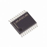
MAX1301BEUP+ Maxim Integrated Products, MAX1301BEUP+ Datasheet - Page 21

MAX1301BEUP+
Manufacturer Part Number
MAX1301BEUP+
Description
IC ADC 16BIT SER 4CH LP 20TSSOP
Manufacturer
Maxim Integrated Products
Datasheet
1.MAX1301BEUPT.pdf
(32 pages)
Specifications of MAX1301BEUP+
Number Of Bits
16
Sampling Rate (per Second)
115k
Data Interface
MICROWIRE™, QSPI™, Serial, SPI™
Number Of Converters
1
Power Dissipation (max)
105.5mW
Voltage Supply Source
Analog and Digital
Operating Temperature
-40°C ~ 85°C
Mounting Type
Surface Mount
Package / Case
20-TSSOP
Lead Free Status / RoHS Status
Lead free / RoHS Compliant
Communication with the MAX1300/MAX1301 is accom-
plished using the three input data word formats shown
in Table 3. Each input data word begins with a start bit.
The start bit is defined as the first high bit clocked into
DIN with CS low when any of the following are true:
• Data conversion is not in process and all data from
• The device is configured for operation in external
• The device is configured for operation in external
• The device is configured for operation in internal
Figure 9. Common-Mode Voltage vs. Input Voltage (FSR = 3 x V
Figure 11. Common-Mode Voltage vs. Input Voltage (FSR = 12 x V
8- and 4-Channel, ±3 x V
the previous conversion has clocked out of DOUT.
clock mode (mode 0) and previous conversion-result
bits B15–B3 have clocked out of DOUT.
acquisition mode (mode 1) and previous conversion-
result bits B15–B7 have clocked out of DOUT.
clock mode, (mode 2) and previous conversion-
result bits B15–B4 have clocked out of DOUT.
-12
-16
-12
-16
12
12
-4
-8
-4
-8
8
4
0
8
4
0
-18
-18
______________________________________________________________________________________
-12
-12
INPUT VOLTAGE (V)
INPUT VOLTAGE (V)
-6
-6
0
0
6
6
12
12
18
18
Start Bit
REF
REF
)
)
Output data is clocked out of DOUT in offset binary for-
mat on the falling edge of SCLK, MSB first (B15). For
output binary codes, see the Transfer Function section
and Figures 12, 13, and 14.
Each analog input has two configurable parameters:
• Single-ended or true-differential input
• Input voltage range
These parameters are configured using the analog input
configuration byte as shown in Table 2. Each analog
input has a dedicated register to store its input configura-
tion information. The timing diagram of Figure 15 shows
how to write to the analog input configuration registers.
Figure 16 shows DOUT and SSTRB timing.
An ADC’s transfer function defines the relationship
between the analog input voltage and the digital output
code. Figures 12, 13, and 14 show the MAX1300/
MAX1301 transfer functions. The transfer function is
determined by the following characteristics:
• Analog input voltage range
• Single-ended or differential configuration
• Reference voltage
The axes of an ADC transfer function are typically in least
significant bits (LSBs). For the MAX1300/MAX1301, an
LSB is calculated using the following equation:
where N is the number of bits (N = 16) and FSR is the
full-scale range (see Figures 7 and 8).
Figure 10. Common-Mode Voltage vs. Input Voltage (FSR = 6 x V
REF
Serial 16-Bit ADCs
Multirange Inputs,
-12
-16
12
-4
-8
8
4
0
1
-18
LSB
-12
=
INPUT VOLTAGE (V)
-6
2
FSR
N
Configuring Analog Inputs
×
0
×
4 096
Transfer Function
.
V
Output Data Format
6
REF
V
12
18
REF
21
)


