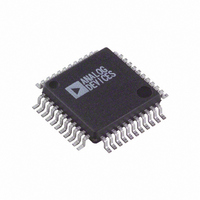
AD9260AS Analog Devices Inc, AD9260AS Datasheet - Page 36

AD9260AS
Manufacturer Part Number
AD9260AS
Description
IC ADC CMOS 16BIT OVRSAMP 44MQFP
Manufacturer
Analog Devices Inc
Datasheet
1.AD9260ASZRL.pdf
(44 pages)
Specifications of AD9260AS
Rohs Status
RoHS non-compliant
Number Of Bits
16
Sampling Rate (per Second)
20M
Data Interface
Parallel
Number Of Converters
1
Power Dissipation (max)
585mW
Voltage Supply Source
Analog and Digital
Operating Temperature
-40°C ~ 85°C
Mounting Type
Surface Mount
Package / Case
44-MQFP, 44-PQFP
Available stocks
Company
Part Number
Manufacturer
Quantity
Price
Company:
Part Number:
AD9260ASZ
Manufacturer:
ADI
Quantity:
100
Company:
Part Number:
AD9260ASZ
Manufacturer:
Analog Devices Inc
Quantity:
10 000
Part Number:
AD9260ASZ
Manufacturer:
ADI/亚德诺
Quantity:
20 000
Company:
Part Number:
AD9260ASZRL
Manufacturer:
Analog Devices Inc
Quantity:
10 000
AD9260
EVALUATION BOARD GENERAL DESCRIPTION
The AD9260 Evaluation Board is designed to provide an easy
and flexible method of exercising the AD9260 and demonstrate
its performance to data sheet specifications. The evaluation
board is fabricated in four layers: the component layer, the
ground layer, the power layer, and the solder layer. The board is
clearly labeled to provide easy identification of components.
Ample space is provided near the analog and clock inputs to
provide additional or alternate signal conditioning.
FEATURES AND USER CONTROLS
Jumper Controlled Mode/OSR Selection
The choice of Mode/OSR can easily be varied by jumping either
JP1, JP2, JP3, or JP4 as illustrated in Figure 78 within the
Mode/OSR Control Block. To obtain the desired mode, refer to
Table 16.
Table 16. AD9260 Evaluation Board Mode Select
Mode/OSR
1×
2×
4×
8×
Selectable Power Bias
The power consumption of the AD9260 can be scaled down if
the user is able to operate the device at a lower clock frequency.
As illustrated in Figure 78, pin cups are provided for the
external resistor (R2) tied to the BIAS pin of the AD9260.
Table 17 defines the recommended resistance for a given clock
speed to obtain the desired power consumption.
1KPOT
8
7
6
5
Connect Jumper
JP4
JP2
JP3
JP1
2.5/3V
NC
VOUT
TRIM
1V
AD780R
U5
15kΩ
10kΩ
GNDS
TEMP
R3
R4
+VIN
NC
15kΩ
10kΩ
1
2
3
4
R12
R13
Figure 77. Evaluation Board External Reference Circuitry
0.1µF
AGND
C18
JP10
49.9Ω
0.1µF
R11
10µF
C19
C17
Rev. C | Page 36 of 44
+
0.1µF
C15
R10
1kΩ
AGND
VCC2
AD817R
Table 17. Evaluation Board Recommended Resistance Value
for External Bias Resistor
Resistor Value
2 kΩ
4 kΩ
8 kΩ
16 kΩ
Data Interfacing Controls
The data interfacing controls (RESETB, CSB, READ, DAV) are
all accessible via SMA connectors (J2–J5) as illustrated in
Figure 78 within the data interfacing control block. The
RESETB, CSB, and READ connections are each supplied with
two sets or resistor pin cups to allow the user to pull-up or pull-
down each signal to a fixed state. R5, R6, and R30 will terminate
to ground, while R7, R28, and R29 terminate to DRVDD. The
DAV and OTR signals are also directly connected to the data
output connector P1. All interfacing controls are buffered
through the CMOS line driver 74HC541.
Buffered Output Data
The twos complement output data is buffered through two
CMOS noninverting bus transceivers (U2 and U3) and made
available at pin connector P1 as illustrated in Figure 78 within
the data output block.
Jumper Controlled Reference Source
The choice of reference for the AD9260 can easily be varied
between 1.0 V, 2.5 V or external by using jumpers JP5, JP6, JP7,
and JP9 as illustrated in Figure 78 within the reference
configuration block. To obtain the desired reference, see
Table 18.
VCC2
U6
0.1µF
C14
1kΩ
R9
Clock Speed (max)
20 MHz
10 MHz
5 MHz
2.5 MHz
AGND
R8
390Ω
Q1
2N2222
C12
0.1µF
585 mW
325 mW
200 mW
150 mW
Power Consumption
+
C13
10µF
VREFEXT


