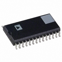
AD1870AR-REEL Analog Devices Inc, AD1870AR-REEL Datasheet - Page 12

AD1870AR-REEL
Manufacturer Part Number
AD1870AR-REEL
Description
IC ADC STEREO 5V 16BIT 28SOIC
Manufacturer
Analog Devices Inc
Datasheet
1.AD1870AR.pdf
(20 pages)
Specifications of AD1870AR-REEL
Rohs Status
RoHS non-compliant
Number Of Bits
16
Sampling Rate (per Second)
48k
Data Interface
I²S, Serial
Number Of Converters
2
Power Dissipation (max)
315mW
Voltage Supply Source
Analog and Digital
Operating Temperature
-40°C ~ 85°C
Mounting Type
Surface Mount
Package / Case
28-SOIC (0.300", 7.50mm Width)
AD1870
Serial Port Data Timing Sequences
The RDEDGE input (Pin 6) selects the bit clock (BCLK) polarity.
RDEDGE HI causes data to be transmitted on the BCLK falling
edge and valid on the BCLK rising edge; RDEDGE LO causes
data to be transmitted on the BCLK rising edge and valid on
the BCLK falling edge. This is shown in the serial data output
timing diagrams. The term “sampling” is used generically to
denote the BCLK edge (rising or falling) on which the serial data is
valid. The term “transmitting” is used to denote the other BCLK
edge. The S/M input (Pin 7) selects Slave Mode (S/M HI) or
Master Mode (S/M LO). Note that in Slave Mode, BCLK may be
continuous or gated, i.e., a stream of pulses during the data phase
followed by periods of inactivity between channels.
In the Master Modes, the bit clock (BCLK), the left/right clock
(LRCK), and the word clock (WCLK) are always outputs, gen-
erated internally in the AD1870 from the master clock (CLKIN)
input. In Master Mode, a LRCK cycle defines a 64-bit “frame.”
LRCK is HI for a 32-bit “field” and LRCK is LO for a 32-
bit “field.”
In the Slave Modes, the bit clock (BCLK) and the left/right clock
(LRCK) are user-supplied inputs. The word clock (WCLK) is an
internally generated output, except when S/M is HI, RLJUST is
HI, and MSBDLY is LO when it is a user-supplied input that
controls the data position. Note that the AD1870 does not sup-
port asynchronous operation in Slave Mode; the clocks
(CLKIN, LRCK, BCLK, and WCLK) must be externally
derived from a common source. In general, CLKIN should be
divided down externally to create LRCK, BCLK, and WCLK.
In the Slave Modes, the relationship between LRCK and BCLK
is not fixed to the extent that there can be an arbitrary number
of BCLK cycles between the end of the data transmission and
the next LRCK transition. The Slave Mode timing diagrams are
therefore simplified as they show precise 32-bit fields and
64-bit frames.
In two Slave Modes, it is possible to pack two 16-bit samples in
a single 32-bit frame, as shown in Figures 15 and 16. BCLK,
LRCK, DATA, and TAG operate at one-half the frequency
(twice the period) as in the 64-bit frame modes. This 32-Bit
Frame Mode is enabled by pulsing the LRCK HI for a mini-
mum of one BCLK period to a maximum of 16 BCLK periods.
–12–
The LRCK HI for one BCLK period case is shown in Figures 15
and 16. With a one or two BCLK period HI pulse on LRCK,
note that both the left and right TAG Bits are output immedi-
ately, back to back. With a three-to-sixteen BCLK period HI pulse
on LRCK, the left TAG Bits are followed by one to fourteen
“dead” cycles, i.e., zeros, followed by the right TAG Bits. Also
note that WCLK stays HI continuously when the AD1870 is
in the 32-Bit Frame Mode. Figure 15 illustrates the left-justified
case, while Figure 16 illustrates the I
In all modes, the left and right channel data is updated with the
next sample within the last 1/8 of the current conversion cycle, i.e.,
within the last four BCLK cycles in 32-Bit Frame Mode, and
within the last eight BCLK cycles in 64-Bit Frame Mode. The
user must constrain the output timing such that the MSB of the
right channel is read before the final 1/8 of the current con-
version period.
Two modes deserve special discussion. The first special mode,
Slave Mode, Data Position Controlled by WCLK Input
(S/M = HI, RLJUST = HI, MSBDLY = LO), shown in
Figure 8, is the only mode in which WCLK is an input. The
16-bit output data-words can be placed at user-defined loca-
tions within 32-bit fields. The MSB will appear in the BCLK
period after WCLK is detected HI by the BCLK sampling edge.
If WCLK is HI during the first BCLK of the 32-bit field, i.e, if
WCLK is tied HI, then the MSB of the output word will be
valid on the sampling edge of the second BCLK. The effect is to
delay the MSB for one bit clock cycle into the field, making the
output data compatible at the data format level with the I
format. Note that the relative placement of the WCLK input
can vary from 32-bit field to 32-bit field, even within the
same 64-bit frame. For example, within a single 64-bit frame,
the left word could be right-justified (by pulsing WCLK HI on
the 16th BCLK) and the right word could be in an I
ible data format (by having WCLK HI at the beginning of the sec-
ond field).
In the second special mode, Master Mode, Right-Justified
with MSB Delay, WCLK Pulsed in 17th BCLK Cycle (S/M
= LO, RLJUST = HI, MSBDLY = LO), shown in Figure 12,
WCLK is an output and is pulsed for one cycle by the AD1870.
The MSB is valid on the 18th BCLK sampling edge, and the
LSB extends into the first BCLK period of the next 32-bit field.
2
S-justified case.
2
S compat-
REV. A
2
S data


