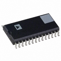
AD1870AR-REEL Analog Devices Inc, AD1870AR-REEL Datasheet - Page 7

AD1870AR-REEL
Manufacturer Part Number
AD1870AR-REEL
Description
IC ADC STEREO 5V 16BIT 28SOIC
Manufacturer
Analog Devices Inc
Datasheet
1.AD1870AR.pdf
(20 pages)
Specifications of AD1870AR-REEL
Rohs Status
RoHS non-compliant
Number Of Bits
16
Sampling Rate (per Second)
48k
Data Interface
I²S, Serial
Number Of Converters
2
Power Dissipation (max)
315mW
Voltage Supply Source
Analog and Digital
Operating Temperature
-40°C ~ 85°C
Mounting Type
Surface Mount
Package / Case
28-SOIC (0.300", 7.50mm Width)
REV. A
(
The flexible serial output port produces data in two’s complement,
MSB-first format. The input and output signals are TTL
compatible. The port is configured by pin selections. Each 16-bit
output word of a stereo pair can be formatted within a 32-bit
field of a 64-bit frame as either right-justified, I
word clock controlled, or left-justified positions. Both 16-bit
samples can also be packed into a 32-bit frame, in left-justified
and I
The AD1870 is fabricated on a single monolithic integrated circuit
using a 0.5 µm CMOS double polysilicon, double metal process
and is offered in a plastic 28-lead SOIC package. Analog and
digital supply connections are separated to isolate the analog
circuitry from the digital supply and reduce digital crosstalk.
The AD1870 operates from a single 5 V power supply over the
temperature range of –40°C to +85°C and typically consumes
less than 260 mW of power.
THEORY OF OPERATION
The stereo, internally differential, analog modulator of the
AD1870 employs a proprietary feedforward and feedback archi-
tecture that passes input signals in the audio band with a unity
transfer function yet simultaneously shapes the quantization
noise generated by the one-bit comparator out of the audio
band (see Figure 1). Without the - architecture, this quanti-
zation noise would be spread uniformly from dc to one-half
the oversampling frequency, 64 × f
Continued from Page 1
V
- Modulator Noise Shaping
IN
TPC 7. Digital Filter Signal Transfer Function to f
Figure 1. Modulator Noise Shaper (One Channel)
2
DIFFERENTIAL
CONVERTER
–100
–110
–120
S compatible positions.
SINGLE-TO-
–10
–20
–30
–40
–50
–60
–70
–80
–90
10
0
0.0
0.1
0.2
)
V
V
IN
IN
0.3
NORMALIZED
0.4
0.5
S
.
0.6
f
S
0.7
0.8
DAC
DAC
2
S compatible,
0.9
MODULATOR
BITSTREAM
OUTPUT
1.0
S
–7–
in a nonuniform manner. Through careful design, this transfer
function can be specified to high-pass filter the quantization
noise out of the audio band into higher frequency regions. The
AD1870 also incorporates a feedback resonator from the fourth
integrator’s output to the third integrator’s input. This resona-
tor does not affect the signal transfer function but allows the
flexible placement of a zero in the noise transfer function for
more effective noise shaping.
Oversampling by 64 simplifies the implementation of a high
performance audio analog-to-digital conversion system. Antialias
requirements are minimal; a single pole of filtering will usually
suffice to eliminate inputs near f
A fourth order architecture was chosen both to strongly shape
the noise out of the audio band and to help break up the idle
tones produced in all - architectures. These architectures
have a tendency to generate periodic patterns with a constant dc
input, a response that looks like a tone in the frequency domain.
These idle tones have a direct frequency dependence on the input
dc offset and an indirect dependence on temperature and time
as it affects the dc offset. The AD1870 suppresses idle tones 20
dB or better below the integrated noise floor.
The AD1870’s modulator was designed, simulated, and ex-
haustively tested to remain stable for any input within a wide
tolerance of its rated input range. The AD1870 is designed to
internally reset itself should it ever be overdriven, to prevent it
from going unstable. It will reset itself within 5 µs at a 48 kHz
sampling frequency after being overdriven. Overdriving the inputs
will produce a waveform “clipped” to plus or minus full scale.
See TPCs 1 through 6 for illustrations of the AD1870’s typical
analog performance as measured by an Audio Precision System
One. Signal-to-(distortion + noise) is shown under a range of
conditions. Note that there is a small variance between the
AD1870 analog performance specifications and some of the
performance plots. This is because the Audio Precision System
One measures THD and noise over a 20 Hz to 24 kHz band-
width, while the analog performance is specified over a 20 Hz to
20 kHz bandwidth (i.e., the AD1870 performs slightly better
than the plots indicate). The power supply rejection graph (TPC 5)
illustrates the benefits of the AD1870’s internal differential ar-
chitecture. The excellent channel separation shown in TPC 6 is
the result of careful chip design and layout.
Digital Filter Characteristics
The digital decimator accepts the modulator’s stereo bit stream
and simultaneously performs two operations on it. First, the
decimator low-pass filters the quantization noise that the modu-
lator shaped to high frequencies and filters any other out-of-
audio-band input signals. Second, it reduces the data rate to an
output word rate equal to f
decimated to stereo 16-bit words at 48 kHz (or other desired
f
frequency components of the bit stream are attenuated by at
least 90 dB.
The AD1870 decimator implements a symmetric finite impulse
response (FIR) filter that possesses a linear phase response.
This filter achieves a narrow transition band (0.1 × f
stop-band attenuation (>90 dB), and low pass-band ripple
(<0.006 dB). The narrow transition band allows the unattenu-
ated digitization of 20 kHz input signals with f
S
- architectures “shape” the quantization noise-transfer function
). The out-of-band one-bit quantization noise and other high
S
. The high frequency bit stream is
S
and its higher multiples.
S
AD1870
as low as
S
), high


