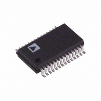
AD9066ARS-REEL Analog Devices Inc, AD9066ARS-REEL Datasheet - Page 2

AD9066ARS-REEL
Manufacturer Part Number
AD9066ARS-REEL
Description
IC ADC 6BIT DUAL 60MSPS 28-SSOP
Manufacturer
Analog Devices Inc
Datasheet
1.AD9066ARS.pdf
(7 pages)
Specifications of AD9066ARS-REEL
Rohs Status
RoHS non-compliant
Number Of Bits
6
Sampling Rate (per Second)
60M
Data Interface
Parallel
Number Of Converters
2
Power Dissipation (max)
600mW
Voltage Supply Source
Analog and Digital
Operating Temperature
-40°C ~ 85°C
Mounting Type
Surface Mount
Package / Case
28-SSOP (0.200", 5.30mm Width)
AD9066–SPECIFICATIONS
ELECTRICAL CHARACTERISTICS
Parameter
ANALOG INPUT
SWITCHING PERFORMANCE
DYNAMIC PERFORMANCE
ENCODE INPUT
DIGITAL OUTPUTS
POWER SUPPLY
NOTES
1
2
3
4
Specifications subject to change without notice.
For ac coupled applications, the ADC is internally biased to insure that the midpoint transition of the ADC is within the limits specified with no signal applied. For
t
Effective number of bits (ENOB) and THD are measured using a FFT with a pure sine wave analog input @ 15.5 MHz, 1 dB below full scale. ENOB is calculated by
Typical thermal impedance for the “R” style (SOIC) 28-lead package is: θ
dc coupled applications, the dc value of the midpoint transition voltage will track the supply voltage within the limits shown for dc input (midscale) plus the dc offset.
Power Supply Rejection Ratio (PSRR) refers to the variation of the input signal range (gain) to supply voltage.
the dc load will not exceed ± 40 µA.
ENOB = (SNR – 1.76 dB)/6.02; THD is measured from full scale to the sum of the second through seventh harmonic of the input.
θ
V
JC
Full-Scale Input Range
Gain Matching (FS Range)
DC Input (Midscale)
Input Offset
Input Capacitance
Input Resistance (DC)
Input Bandwidth (3 dB)
Gain Flatness (to 15 MHz)
Integral Linearity
Differential Linearity
Monotonicity
Max Conversion Rate
Output Delay (t
Output Delay (t
Aperture Uncertainty (Jitter)
Aperture Time (t
Effective Number of Bits
SINAD
Harmonic Distortion (THD)
Crosstalk Rejection
Logic High Voltage
Logic Low Voltage
Input High Current
Input Low Current
Pulsewidth High
Pulsewidth Low
Output Coding
Logic High Voltage (I
Logic Low Voltage (I
+V
Power Supply Rejection Ratio
+V
Power Dissipation
and t
= 26.97°C/W, θ
S
S
PD
Supply Voltage
Supply Current
are measured from the 1.4 V level of the Clock and the 50% level between V
1
CA
V
PD
= 51.61°C/W, θ
)
A
2
)
)
4
2
1
OL
OH
= 1 mA)
= 1 mA)
3
JA
1
= 78.58°C/W.
Test
Level
IV
V
VI
IV
VI
V
V
IV
IV
V
V
VI
VI
VI
IV
VI
VI
VI
VI
VI
IV
VI
VI
VI
VI
VI
VI
VI
VI
IV
IV
VI
(+V
S
Temp
Full
Full
+25°C
Full
Full
Full
+25°C
+25°C
Full
Full
Full
Full
Full
Full
+25°C
+25°C
+25°C
+25°C
+25°C
+25°C
Full
Full
Full
Full
Full
Full
Full
Full
Full
Full
Full
Full
Full
= +5 V, AIN = 15.5 MHz, Encode Rate = 60 MSPS, T
JC
= 4°C/W, θ
Min
475
–1.0
25
60
4
5.3
34
40
40
2.0
7.0
7.0
3.8
4.75
–1.0
–0.5
AD9066JR
OH
Offset Binary
Guaranteed
CA
Typ
500
+V
10
45
100
0.25
10
1.0
5.7
36
50
50
110
80
400
and V
= 41°C/W, θ
S
– 1.1
OL
. The ac load on all the digital outputs during test is 10 pF (max),
JA
Max
525
16
+1.0
15
55
+1.0
+0.5
11
0.8
500
500
0.4
5.25
130
120
600
= 45°C/W, and the “RS” style (SSOP) 28-lead package is:
Min
450
–1.0
22
–1.0
–0.5
60
4
5.2
33
40
40
2.0
7.0
7.0
3.8
4.75
AD9066AR/ARS
C
= T
Guaranteed
Offset Binary
Typ
+V
10
45
100
0.25
10
1.0
5.7
36
50
50
110
80
400
500
A
)
S
– 1.1
Max
530
16
+1.0
15
57
+1.0
+0.5
12
0.8
500
500
0.4
5.25
130
120
600
Unit
mV
mV
V
LSBs
pF
kΩ
MHz
dB
LSBs
LSBs
MSPS
ns
ns
ps rms
ns
Bits
dB
dB
dBc
V
V
µA
µA
ns
ns
V
V
V
mV/V
mA
mW


