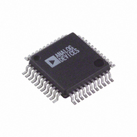
AD9260ASRL Analog Devices Inc, AD9260ASRL Datasheet - Page 38

AD9260ASRL
Manufacturer Part Number
AD9260ASRL
Description
IC ADC 16BIT 2.5MHZ 44-MQFP T/R
Manufacturer
Analog Devices Inc
Datasheet
1.AD9260ASZRL.pdf
(44 pages)
Specifications of AD9260ASRL
Rohs Status
RoHS non-compliant
Number Of Bits
16
Sampling Rate (per Second)
20M
Data Interface
Parallel
Number Of Converters
1
Power Dissipation (max)
585mW
Voltage Supply Source
Analog and Digital
Operating Temperature
-40°C ~ 85°C
Mounting Type
Surface Mount
Package / Case
44-MQFP, 44-PQFP
AD9260
APPLICATION INFORMATION
1.
2.
3.
4.
5.
6.
The ADC analog input should not be overdriven. Using a
signal amplitude slightly lower than FSR will allow a small
amount of headroom so that noise or DC offset voltage will
not overrange the ADC and hard limit on signal peaks.
Two-tone tests can produce signal envelopes that exceed
FSR. Set each test signal to slightly less than –6 dB to
prevent hard limiting on peaks.
Band-pass filtering of test signal generators is absolutely
necessary for SNR, THD, and IMD tests. Note that a low
noise signal generator along with a high Q band-pass filter
is often necessary to achieve the attainable noise
performance of the AD9260.
Test signal generators must have exceptional noise
performance to achieve accurate SNR measurements.
Good generators, together with fifth-order elliptical band-
pass filters, are recommended for SNR tests. Narrow
bandwidth crystal filters can also be used to filter generator
broadband noise, but they should be carefully tested for
operation at high signal levels.
The analog inputs of the AD9260 should be terminated
directly at the input pin sockets with the correct filter
terminating impedance (50 Ω or 75 Ω), or it should be
driven by a low output impedance buffer. Short leads are
necessary to prevent digital noise pickup.
A low noise (jitter) clock signal generator is required for
good ADC dynamic performance. A poor generator can
seriously impair good SNR performance particularly at
higher input frequencies. A high frequency generator,
based on a clock source (e.g., crystal source), is
recommended. Frequency-synthesized clock generators
should generally be avoided because they typically provide
Rev. C | Page 38 of 44
7.
8.
9.
10. Prototype plug-boards or wire-wrap boards will not
poor jitter performance. See Note 8 if a crystal-based clock
generator is used during FFT testing.
A low jitter clock may be generated by using a high-
frequency clock source and dividing this frequency down
with a low noise clock divider to obtain the AD9260 input
CLK. Maintaining a large amplitude clock signal may also
be very beneficial in minimizing the effects of noise in the
digital gates of the clock generation circuitry.
Finally, special care should be taken to avoid coupling
noise into any digital gates preceding the AD9260 CLK pin.
Short leads are necessary to preserve fast rise times and
careful decoupling should be used with these digital gates
and the supplies for these digital gates should be connected
to the same supplies as that of the internal AD9260 clock
circuitry (Pins 44 and 38).
Two-tone testing will require isolation between test signal
generators to prevent IMD generation in the test generator
output circuits.
A very low-side lobe window must be used for FFT
calculations if generators cannot be phase-locked and set to
exact frequencies.
A well designed, clean PC board layout will assure proper
operation and clean spectral response. Proper grounding
and bypassing, short lead lengths, separation of analog and
digital signals, and the use of ground planes are
particularly important for high frequency circuits.
Multilayer PC boards are recommended for best
performance, but if carefully designed, a two-sided PC
board with large heavy (20 oz. foil) ground planes can give
excellent results.
be satisfactory.


