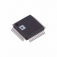
AD7621AST Analog Devices Inc, AD7621AST Datasheet - Page 6

AD7621AST
Manufacturer Part Number
AD7621AST
Description
IC ADC 16BIT 2MSPS DIFF 48LQFP
Manufacturer
Analog Devices Inc
Series
PulSAR®r
Datasheet
1.AD7621ACPZRL.pdf
(32 pages)
Specifications of AD7621AST
Number Of Bits
16
Sampling Rate (per Second)
2M
Data Interface
Serial, Parallel
Number Of Converters
1
Power Dissipation (max)
86mW
Voltage Supply Source
Analog and Digital
Operating Temperature
-40°C ~ 85°C
Mounting Type
Surface Mount
Package / Case
48-LQFP
For Use With
EVAL-AD7621CBZ - BOARD EVALUATION FOR AD7621
Lead Free Status / RoHS Status
Contains lead / RoHS non-compliant
Available stocks
Company
Part Number
Manufacturer
Quantity
Price
Company:
Part Number:
AD7621AST
Manufacturer:
ADI
Quantity:
260
Company:
Part Number:
AD7621ASTZ
Manufacturer:
Analog Devices Inc
Quantity:
10 000
Part Number:
AD7621ASTZ
Manufacturer:
ADI/亚德诺
Quantity:
20 000
Company:
Part Number:
AD7621ASTZRL
Manufacturer:
Analog Devices Inc
Quantity:
10 000
AD7621
Parameter
SLAVE SERIAL INTERFACE MODES
1
2
3
4
5
6
SERIAL CLOCK TIMING SPECIFICATIONS
Table 4. Serial Clock Timings in Master Read After Convert Mode
DIVSCLK[1]
DIVSCLK[0]
SYNC to SCLK First Edge Delay Minimum
Internal SCLK Period Minimum
Internal SCLK Period Maximum
Internal SCLK High Minimum
Internal SCLK Low Minimum
SDOUT Valid Setup Time Minimum
SDOUT Valid Hold Time Minimum
SCLK Last Edge to SYNC Delay Minimum
BUSY High Width Maximum (Wideband and Warp Modes)
BUSY High Width Maximum (Normal Mode)
BUSY High Width Maximum (Impulse Mode)
See the Conversion Control section.
All timings for wideband warp mode are the same as warp mode.
In warp mode only, the time between conversions is 1 ms; otherwise, there is no required maximum time.
See the Digital Interface, and RESET sections.
In serial interface modes, the SYNC, SCLK, and SDOUT timings are defined with a maximum load C
In serial master read during convert mode. See Table 4 for serial master read after convert mode timing specifications.
External SCLK Setup Time
External SCLK Active Edge to SDOUT Delay
SDIN Setup Time
SDIN Hold Time
External SCLK Period
External SCLK High
External SCLK Low
TO OUTPUT
NOTE
IN SERIAL INTERFACE MODES, THE SYNC, SCLK AND
SDOUT ARE DEFINED WITH A MAXIMUM LOAD.
C
L
Figure 2. Load Circuit for Digital Interface Timing,
OF 10pF; OTHERWISE, THE LOAD IS 60pF MAXIMUM.
SDOUT, SYNC, and SCLK Outputs, C
PIN
50pF
C
L
500μA
500μA
5
I
I
OL
OH
(Refer to Figure 40 and Figure 41)
1.4V
L
= 10 pF
Rev. 0 | Page 6 of 32
Symbol
t
t
t
t
t
t
t
t
t
t
t
18
19
19
20
21
22
23
24
28
28
28
Symbol
t
t
t
t
t
t
t
31
32
33
34
35
36
37
L
of 10 pF; otherwise, the load is 60 pF maximum.
t
DELAY
0.8V
0
0
0.5
8
12
2
3
1
0
0
0.500
0.650
0.780
Min
5
1
5
5
12.5
5
5
Figure 3. Voltage Reference Levels for Timing
0
1
3
16
25
6
7
5
0.5
0.5
0.720
0.870
1.000
2V
0.8V
Typ
1
0
3
32
50
15
16
5
10
9
1.160
1.310
1.440
2V
Max
8
1
1
3
64
100
31
32
5
28
26
2.040
2.190
2.320
t
DELAY
2V
0.8V
Unit
ns
ns
ns
ns
ns
ns
ns
ns
μs
μs
μs
Unit
ns
ns
ns
ns
ns
ns
ns


