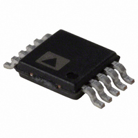
AD7992BRM-1 Analog Devices Inc, AD7992BRM-1 Datasheet - Page 22

AD7992BRM-1
Manufacturer Part Number
AD7992BRM-1
Description
IC ADC 12BIT 2CHAN I2C 10MSOP
Manufacturer
Analog Devices Inc
Datasheet
1.AD7992BRMZ-1.pdf
(28 pages)
Specifications of AD7992BRM-1
Number Of Bits
12
Sampling Rate (per Second)
79k
Data Interface
I²C, Serial
Number Of Converters
1
Power Dissipation (max)
2.2mW
Voltage Supply Source
Single Supply
Operating Temperature
-40°C ~ 125°C
Mounting Type
Surface Mount
Package / Case
10-TFSOP (0.118", 3.00mm Width)
For Use With
EVAL-AD7992CB - BOARD EVALUATION FOR AD7992
Lead Free Status / RoHS Status
Contains lead / RoHS non-compliant
AD7992
WRITING TWO BYTES OF DATA TO A LIMIT
REGISTER OR HYSTERESIS REGISTER
Each of the limit registers and hysteresis registers are 12-bit
registers, so two bytes of data are required to write a value to
any one of them. Writing two bytes of data to one of these
registers consists of the serial bus write address, the chosen
limit register address written to the address pointer register,
followed by two data bytes written to the selected data register.
See Figure 27.
SDA (CONTINUED)
SCL (CONTINUED)
SDA
SCL
START BY
MASTER
MOST SIGNIFICANT DATA BYTE
9
0
1
0
1
0
1
SERIAL BUS ADDRESS BYTE
0
0
A3
0
FRAME 1
D11
A2
Figure 27. Two-Byte Write Sequence
D10
A1
Rev. 0 | Page 22 of 28
A0
D9
R/W
D8
ACK. BY
AD7992
ACK. BY
AD7992
9
9
If the master is write-addressing the AD7992, it can write to
more than one register with out re-addressing the ADC. After
the first write operation has completed for the first data register,
during the next byte, the master writes to the address pointer
byte to select the next data register for a write operation. This
eliminates the need to re-address the device in order to write to
another data register.
C4
D7
1
1
LEAST SIGNIFICANT DATA BYTE
C3
D6
ADDRESS POINTER REGISTER
C2
D5
D4
C1
FRAME 2
D3
P3
P2
D2
D1/0
P1
D0/0
P0
ACK. BY
ACK. BY
AD7992
AD7992
9
9
STOP BY
MASTER


