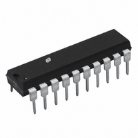
ADC08061CIN National Semiconductor, ADC08061CIN Datasheet - Page 13

ADC08061CIN
Manufacturer Part Number
ADC08061CIN
Description
IC CONVERTER 500 NS A/D 20-DIP
Manufacturer
National Semiconductor
Datasheet
1.ADC08061CIN.pdf
(16 pages)
Specifications of ADC08061CIN
Number Of Bits
8
Sampling Rate (per Second)
300k
Number Of Converters
1
Power Dissipation (max)
100mW
Voltage Supply Source
Single Supply
Operating Temperature
-40°C ~ 85°C
Mounting Type
Through Hole
Package / Case
20-DIP (0.300", 7.62mm)
Lead Free Status / RoHS Status
Contains lead / RoHS non-compliant
Other names
*ADC08061CIN
Available stocks
Company
Part Number
Manufacturer
Quantity
Price
Application Information
shows the input code needed to select a given channel The
multiplexer address is latched when received but the multi-
plexer channel is updated after the completion of the cur-
rent conversion
The multiplexer address data must be valid at the time of
RD’s falling edge remain valid during the conversion and
can go high after RD goes high when operating in the Read
Mode
The multiplexer address data should be valid at or before
the time of WR’s falling edge remain valid while WR is low
and go invalid after WR goes high when operating in the
WR-RD Mode
3 0 REFERENCE INPUTS
The two V
tial and define the zero to full-scale input range of the A to D
converter This allows the designer to vary the span of the
analog input since this range will be equivalent to the volt-
age difference between V
with minimum output voltages above GND can also be com-
pensated by connecting V
this minimum voltage By reducing V
b
can be increased (i e
9 8 mV) The ADC08061 2’s reference arrangement also
facilitates ratiometric operation and in many cases the
ADC08061 2’s power supply can be used for transducer
power as well as the V
achieved by connecting V
V
ADC08061 2’s linearity degrades when V
is less than 2 0V
The voltage at V
digital output of all zeros Though V
the reference design affords nearly differential-input capability
for some measurement applications Figure 6 shows one
possible differential configuration
It should be noted that while the two V
differential the digital output will be zero for any analog in-
put voltage if V
Represents a multiplexer channel in the ADC08062
REF
V
REF
a
and a transducer’s power supply input to V
b
ADC08062
) to less than 5V the sensitivity of the converter
REF
TABLE I Multiplexer Addressing
A0
0
1
inputs of the ADC08061 2 are fully differen-
REF
REF
b
b
t
REF
sets the input level that produces a
V
if V
REF
REF
REF
REF
source Ratiometric operation is
FIGURE 6 ADC08061 and ADC08062 Equivalent Input Circuit Model
REF
b
a
a
b
to a voltage that is equal to
and V
e
to GND and connecting
IN
2 5V then 1 LSB
is not itself differential
REF
REF
REF
(Continued)
Channel
REF
(V
V
V
b
REF
IN1
IN2
inputs are fully
a
Transducers
b
e
l
V
V
a
REF
REF
The
b
e
a
l
13
4 0 ANALOG INPUT AND SOURCE IMPEDANCE
The ADC08061 2’s analog input circuitry includes an ana-
log switch with an ‘‘on’’ resistance of 70
of 1 4 pF and 12 pF (see Figure 6 ) The switch is closed
during the A D’s input signal acquisition time (while WR is
low when using the WR-RD Mode) A small transient current
flows into the input pin each time the switch closes A tran-
sient voltage whose magnitude can increase as the source
impedance increases may be present at the input So long
as the source impedance is less than 500
age transient will not cause errors and need not be filtered
Large source impedances can slow the charging of the
sampling capacitors and degrade conversion accuracy
Therefore only signal sources with output impedances less
than 500
achieved at the minimum sample time (100 ns maximum) A
signal source with a high output impedance should have its
output buffered with an operational amplifier Any ringing or
voltage shifts at the op amp’s output during the sampling
period can result in conversion errors
Correct conversion results will be obtained for input volt-
ages greater than GND
100 mV Do not allow the signal source to drive the analog
input pin more than 300 mV higher than V
300 mV lower than GND The current flowing through any
analog input pin should be limited to 5 mA or less to avoid
permanent damage to the IC if an analog input pin is forced
beyond these voltages The sum of all the overdrive cur-
rents into all pins must be less than 20 mA Some sort of
protection scheme should be used when the input signal is
expected to extend more than 300 mV beyond the power
supply limits A simple protection network using resistors
and diodes is shown in Figure 8
6 0 INHERENT SAMPLE-AND-HOLD
An important benefit of the ADC08061 2’s input architec-
ture is the inherent sample-and-hold (S H) and its ability to
measure relatively high speed signals without the help of an
external S H In a non-sampling converter regardless of its
speed the input must remain stable to at least
throughout the conversion process if full accuracy is to be
maintained Consequently for many high speed signals this
signal must be externally sampled and held stationary dur-
ing the conversion
The ADC08061 and ADC08062 are suitable for DSP-based
systems because of the direct control of the S H through
should be used if rated accuracy is to be
b
100 mV and less than V
http
and capacitance
a
TL H 11086 – 19
the input volt-
or more than
www national com
a
LSB
a


