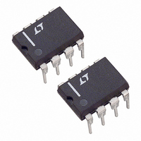
LTC1291DCN8#PBF Linear Technology, LTC1291DCN8#PBF Datasheet - Page 17

LTC1291DCN8#PBF
Manufacturer Part Number
LTC1291DCN8#PBF
Description
IC DATA ACQ SYSTEM 12BIT 8-DIP
Manufacturer
Linear Technology
Type
Data Acquisition System (DAS)r
Datasheet
1.LTC1291DCN8PBF.pdf
(20 pages)
Specifications of LTC1291DCN8#PBF
Resolution (bits)
12 b
Data Interface
Serial, Parallel
Voltage Supply Source
Single Supply
Voltage - Supply
5V
Operating Temperature
0°C ~ 70°C
Mounting Type
Through Hole
Package / Case
8-DIP (0.300", 7.62mm)
Number Of Elements
1
Resolution
12Bit
Architecture
SAR
Sample Rate
54KSPS
Input Polarity
Unipolar
Input Type
Voltage
Rated Input Volt
5V
Differential Input
Yes
Power Supply Requirement
Single
Single Supply Voltage (typ)
5V
Dual Supply Voltage (typ)
Not RequiredV
Dual Supply Voltage (min)
Not RequiredV
Dual Supply Voltage (max)
Not RequiredV
Power Dissipation
500mW
Differential Linearity Error
±1LSB(Typ)
Integral Nonlinearity Error
±0.75LSB
Operating Temp Range
0C to 70C
Operating Temperature Classification
Commercial
Mounting
Through Hole
Pin Count
8
Package Type
PDIP N
Lead Free Status / RoHS Status
Lead free / RoHS Compliant
Sampling Rate (per Second)
-
Lead Free Status / Rohs Status
Compliant
Available stocks
Company
Part Number
Manufacturer
Quantity
Price
RC Input Filtering
It is possible to filter the inputs with an RC network as
shown in Figure 12. For large values of C
capacitive input switching currents are averaged into a net
DC current. A filter should be chosen with a small resistor
and a large capacitor to prevent DC drops across the
resistor. The magnitude of the DC current is approximately
I
When running at the minimum cycle time of 18.5 s, the
input current equals 27 A at V
of 4.5 will cause 0.1LSB of full-scale error. If a large filter
resistor must be used, errors can be reduced by increasing
the cycle time as shown in the Typical Performance
Characteristics curve Maximum Filter Resistor vs Cycle
Time.
A
Input Leakage Current
Input leakage currents also can create errors if the source
resistance gets too large. For example, the maximum input
leakage specification of 1 A (at 125 C) flowing through a
source resistance of 1k will cause a voltage drop of 1mV
or 0.8LSB. This error will be much reduced at lower
temperatures because leakage drops rapidly (see typical
performance characteristics curve Input Channel Leakage
Current vs Temperature).
SAMPLE-AND-HOLD
Single-Ended Input
The LTC1291 provides a built-in sample-and-hold (S/H)
function on the +IN input for signals acquired in the single-
ended mode (–IN pin grounded). The sample-and-hold
DC
PPLICATI
= 100pF • V
V
IN
–
R
FILTER
IN
Figure 12. RC Input Filtering
O
/t
CYC
U
I
DC
S
and is roughly proportional to V
I FOR ATIO
U
C
IN
FILTER
= 5V. Here a filter resistor
“+”
“–”
W
LTC1291
LTC1291 F12
F
(e.g., 1 F) the
U
IN
.
allows the LTC1291 to convert rapidly varying signals (see
typical performance characteristics curve of S/H Acquisition
Time vs Source Resistance). The input voltage is sampled
during the t
interval begins as the bit preceding the MSBF bit is shifted
in and continues until the falling edge of the PS bit is
received. On this falling edge, the S/H goes into the hold
mode and the conversion begins.
Differential Input
With a differential input the A/D no longer converts a single
voltage but converts the difference between two voltages.
The voltage on the +IN pin is sampled and held and can be
rapidly time varying. The voltage on the –IN pin must
remain constant and be free of noise and ripple throughout
the conversion time. Otherwise the differencing operation
will not be done accurately. The conversion time is 12 CLK
cycles. Therefore a change in the –IN input voltage during
this interval can cause conversion errors. For a sinusoidal
voltage on the –IN input this error would be:
Where f
V
CLK. Usually V
signal on the –IN input to generate a 0.25LSB error
(300 V) with the converter running at CLK = 1MHz, its
peak value would have to be 66mV. Rearranging the above
equation, the maximum sinusoidal signal that can be
digitized to a given accuracy is given as:
For 0.25LSB error (300 V), the maximum input sinusoid
with a 5V peak amplitude that can be digitized is 0.8Hz.
PEAK
V
f
(
ERROR MAX
IN
is its peak amplitude and f
)
(–IN)
(
SMPL
V
is the frequency of the –IN input voltage,
ERROR MAX
2 V
)
ERROR
time as shown in Figure 9. The sampling
PEAK
2 f
(
will not be significant. For a 60Hz
(
)
IN PEAK
)
V
f
12
CLK
CLK
is the frequency of the
f
12
CLK
LTC1291
17
1291fa


