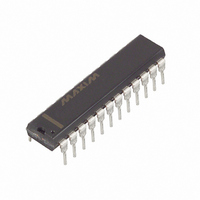
MAX1270ACNG+ Maxim Integrated Products, MAX1270ACNG+ Datasheet - Page 4

MAX1270ACNG+
Manufacturer Part Number
MAX1270ACNG+
Description
IC ADC 12BIT MULTIRANGE 24-DIP
Manufacturer
Maxim Integrated Products
Type
Data Acquisition System (DAS), ADCr
Datasheet
1.MAX1270BCAI.pdf
(20 pages)
Specifications of MAX1270ACNG+
Resolution (bits)
12 b
Sampling Rate (per Second)
100k
Data Interface
Serial
Voltage Supply Source
Single Supply
Voltage - Supply
4.75 V ~ 5.25 V
Operating Temperature
0°C ~ 70°C
Mounting Type
Through Hole
Package / Case
24-DIP (0.300", 7.62mm)
Number Of Adc Inputs
8
Architecture
SAR
Conversion Rate
110 KSPs
Resolution
12 bit
Input Type
Voltage
Interface Type
3-Wire (SPI, QSPI, MICROWIRE)
Voltage Reference
Internal 4.096 V or External
Supply Voltage (max)
5 V
Maximum Power Dissipation
1067 mW
Maximum Operating Temperature
+ 70 C
Mounting Style
Through Hole
Minimum Operating Temperature
0 C
Lead Free Status / RoHS Status
Lead free / RoHS Compliant
ELECTRICAL CHARACTERISTICS (continued)
(V
50% duty cycle (MAX127_B); f
otherwise noted. Typical values are T
Multirange, +5V, 8-Channel,
Serial 12-Bit ADCs
4
INTERNAL REFERENCE
REF Output Voltage
REF Output Tempco
Output Short-Circuit Current
Load Regulation
Capacitive Bypass at REF
Capacitive Bypass at REFADJ
REFADJ Output Voltage
REFADJ Adjustment Range
Buffer Voltage Gain
REFERENCE INPUT (Reference buffer disabled, reference input applied to REF)
Input Voltage Range
Input Current
Input Resistance
REFADJ Threshold for Buffer
Disable
POWER REQUIREMENT
Supply Voltage
Supply Current
Power-Supply Rejection
Ratio (Note 7)
TIMING
External Clock Frequency Range
Acquisition Phase
DD
_______________________________________________________________________________________
= +5.0V ±5%; unipolar/bipolar range; external reference mode, V
PARAMETER
CLK
= 1.8MHz, 50% duty cycle (MAX127_A); 18 clock/conversion cycle, T
A
SYMBOL
TC V
= +25°C.)
PSRR
f
V
V
SCLK
I
REF
DD
DD
REF
T
MAX1270_C/MAX1271_C
MAX1270_E/MAX1271_E
0 to 0.5mA output current (Note 5)
Figure 1
V
V
Normal
STBYPD power-down mode (Note 6)
FULLPD power-down mode
External reference = 4.096V
Internal reference
MAX127_A
MAX127_B
External clock mode
(Note 8)
Internal clock mode, Figure 9
A
REF
REF
= +25°C
= 4.18V
= 4.18V
CONDITIONS
Bipolar range
Unipolar range
Normal or STBYPD
FULLPD
Normal or STBYPD
FULLPD
REF
MAX127_A
MAX127_B
= +4.096V; 4.7µF at REF; external clock; f
4.076
2.465
V
0.01
2.40
4.18
4.75
MIN
4.7
0.5
0.1
0.1
3.3
3.0
DD
10
3
-
4.096
2.500
1.638
±1.5
±0.1
±0.5
±15
±30
700
120
A
TYP
30
6
= T
MIN
4.116
2.535
4.18
5.25
±0.5
MAX
400
850
220
1.8
2.0
to T
10
18
10
1
5
CLK
MAX
= 2.0MHz,
ppm/°C
, unless
UNITS
MHz
LSB
MΩ
mA
mV
V/V
mA
µA
kΩ
µA
µF
µF
µs
%
V
V
V
V
V


