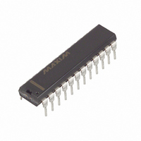
MAX1270ACNG+ Maxim Integrated Products, MAX1270ACNG+ Datasheet - Page 6

MAX1270ACNG+
Manufacturer Part Number
MAX1270ACNG+
Description
IC ADC 12BIT MULTIRANGE 24-DIP
Manufacturer
Maxim Integrated Products
Type
Data Acquisition System (DAS), ADCr
Datasheet
1.MAX1270BCAI.pdf
(20 pages)
Specifications of MAX1270ACNG+
Resolution (bits)
12 b
Sampling Rate (per Second)
100k
Data Interface
Serial
Voltage Supply Source
Single Supply
Voltage - Supply
4.75 V ~ 5.25 V
Operating Temperature
0°C ~ 70°C
Mounting Type
Through Hole
Package / Case
24-DIP (0.300", 7.62mm)
Number Of Adc Inputs
8
Architecture
SAR
Conversion Rate
110 KSPs
Resolution
12 bit
Input Type
Voltage
Interface Type
3-Wire (SPI, QSPI, MICROWIRE)
Voltage Reference
Internal 4.096 V or External
Supply Voltage (max)
5 V
Maximum Power Dissipation
1067 mW
Maximum Operating Temperature
+ 70 C
Mounting Style
Through Hole
Minimum Operating Temperature
0 C
Lead Free Status / RoHS Status
Lead free / RoHS Compliant
Multirange, +5V, 8-Channel,
Serial 12-Bit ADCs
TIMING CHARACTERISTICS
(V
2.0MHz (MAX127_B); f
(Figures 2, 5, 7, 10)
Note 1: Accuracy specifications tested at V
Note 2: External reference: V
Note 3: Ground “on” channel; sine wave applied to all “off” channels. V
Note 4: Guaranteed by design, not production tested.
Note 5: Use static external loads during conversion for specified accuracy.
Note 6: Tested using internal reference.
Note 7: PSRR measured at full scale. Tested for the ±10V (MAX1270) and ±4.096V (MAX1271) input ranges.
Note 8: Acquisition phase and conversion time are dependent on the clock period; clock has 50% duty cycle (Figure 6).
Note 9: Not production tested. Provided for design guidance only.
6
DIN to SCLK Setup
DIN to SCLK Hold
SCLK Fall to Output Data Valid
CS Fall to Output Enable
CS Rise to Output Disable
CS to SCLK Rise Setup
CS to SCLK Rise Hold
SCLK Pulse-Width High
SCLK Pulse-Width Low
SCLK Fall to SSTRB
CS to SSTRB Output Enable
CS to SSTRB Output Disable
SSTRB Rise to SCLK Rise
DD
_______________________________________________________________________________________
= +4.75V to +5.25V; unipolar/bipolar range; external reference mode, V
rejection test.
PARAMETER
CLK
= 1.8MHz (MAX127_A); T
REF
= 4.096V, offset error nulled. Ideal last-code transition = FS - 3/2 LSB.
SYMBOL
t
SSTRB
t
t
t
t
t
t
t
CSH
t
SCK
t
t
t
CSS
t
SDV
STR
DO
DH
CH
DS
DV
TR
CL
DD
= +5.0V. Performance at power-supply tolerance limit is guaranteed by power-supply
C
C
C
C
C
Internal clock mode only (Note 4)
LOAD
LOAD
LOAD
LOAD
LOAD
A
= T
= 100pF
= 100pF
= 100pF
= 100pF, external clock mode only
= 100pF, external clock mode only
MIN
to T
CONDITIONS
MAX
IN
, unless otherwise noted. Typical values are T
= ±5V (MAX1270), V
REF
= +4.096V; 4.7µF at REF; external clock; f
IN
= ±4V (MAX1271).
100
100
200
200
MIN
20
0
0
TYP
MAX
170
120
100
200
200
200
0
A
= +25°C.)
UNITS
CLK
ns
ns
ns
ns
ns
ns
ns
ns
ns
ns
ns
ns
ns
=


