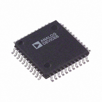
AD2S1200YSTZ Analog Devices Inc, AD2S1200YSTZ Datasheet - Page 14

AD2S1200YSTZ
Manufacturer Part Number
AD2S1200YSTZ
Description
IC CONV R/D 12-BIT W/OSC 44-LQFP
Manufacturer
Analog Devices Inc
Type
R/D Converterr
Datasheet
1.AD2S1200.pdf
(24 pages)
Specifications of AD2S1200YSTZ
Resolution (bits)
12 b
Data Interface
Serial, Parallel
Voltage Supply Source
Analog and Digital
Voltage - Supply
4.75 V ~ 5.25 V
Operating Temperature
-40°C ~ 125°C
Mounting Type
Surface Mount
Package / Case
44-LQFP
Input Channel Type
Differential
Supply Voltage Range - Analog
4.75V To 5.25V
Supply Voltage Range - Digital
4.75V To 5.25V
Lead Free Status / RoHS Status
Lead free / RoHS Compliant
For Use With
EVAL-AD2S1200CBZ - BOARD EVAL FOR AD2S1200
Sampling Rate (per Second)
-
Lead Free Status / RoHS Status
Lead free / RoHS Compliant, Lead free / RoHS Compliant
Available stocks
Company
Part Number
Manufacturer
Quantity
Price
Company:
Part Number:
AD2S1200YSTZ
Manufacturer:
Analog Devices Inc
Quantity:
10 000
AD2S1200
SERIAL INTERFACE
The angular position and angular velocity are available on the
AD2S1200 in two 12-bit registers. These registers can be
accessed via a 3-wire serial interface, SO, RD , and SCLK, that
operates at clock rates up to 25 MHz and is compatible with SPI
and DSP interface standards. The serial interface is selected by
holding low the SOE pin. Data from the position and velocity
integrators are first transferred to the position and velocity
registers, using the SAMPLE pin. The RDVEL polarity pin
selects which register from the position or the velocity registers
is transferred to the output register. The CS pin must be held
low to transfer the selected data register to the output register.
Finally, the RD input is used to read the data that will be
clocked out of the output register and will be available on the
serial output pin, SO. When the serial interface is selected, DB11
is used as the serial output pin, SO, and DB10 is used as the
serial clock input, SCLK, while pins DB0–DB9 are placed in the
high impedance state. The timing requirements for the read
cycle are described in Figure 8.
SO Output
The output shift register is 16-bit wide. Data is shifted out of the
device as a 16-bit word under the control of the serial clock
input, SCLK. The timing diagram for this operation is shown in
Figure 8. The 16-bit word consists of 12 bits of angular data
(position or velocity depending on RDVEL input), one RDVEL
status bit and three status bits, a parity bit, degradation of signal
bit, and loss of tracking bit. Data is read out MSB first (bit 15)
on the SO pin. Bit 15 through bit 4 correspond to the angular
information. The angular position data format is unsigned
binary, with all zeros corresponding to 0 degrees and all ones
corresponding to 360 degrees –l LSB. The angular velocity data
format instead is twos complement binary, with the MSB
representing the rotation direction. Bit 3 is the RDVEL status
bit, 1 indicating position and 0 indicating velocity. Bit 2 is DOS,
the degradation of signal flag (refer to the Fault Detection
Circuit section). Bit 1 is LOT, the loss of tracking flag (refer to
the Fault Detection Circuit section). Bit 0 is PAR, the parity bit:
both position and velocity data are odd parity format; the data
read out will always contain an odd number of logic highs (1s).
Rev. 0 | Page 14 of 24
SAMPLE Input
Data is transferred from the position and velocity integrators,
respectively, to the position and velocity registers following a
high-to-low transition on the SAMPLE signal. This pin must be
held low for at least t
data. RD should not be pulled low before this time since data
would not be ready. The converter will continue to operate
during the read process.
CS Input
The device will be enabled when CS is held low.
RD Input
The 12-bit data bus lines are normally in a high impedance
state. The output buffer is enabled when CS and RD are held
low. The RD input is an edge-triggered input that acts as frame
synchronization signal and output enable. A falling edge of the
RD signal transfers data to the output buffer and data will be
available on the serial output pin, SO. RD must be held low for t
before the data is valid on the outputs. After RD goes low, the
serial data will be clocked out of the SO pin on the falling edges
of the SCLK (after a minimum of t
already available at the SO pin on the very first falling edge of
the SCLK. Each other bit of the data word will be shifted out on
the rising edge of SCLK and will be available at the SO pin on
the falling edge of SCLK for the next 15 clock pulses.
The high-to-low transition of RD must happen during the high
time of the SCLK to avoid MSB being shifted on the first rising
edge of the SCLK and lost. RD may rise high after the falling
edge of the last bit transmitted. Subsequent negative edges
greater than the defined word length will clock zeros from the
data output if RD remains in a low state. If the user is reading
data continuously, RD can be reapplied a minimum of t
it is released.
RDVEL Input
RDVEL input is used to select between the angular position and
velocity registers. RDVEL is held high for angular position and
low for angular velocity. The RDVEL pin must be set (stable) at
least t
4
ns before the RD pin is pulled low.
1
ns to guarantee correct latching of the
10
ns): the MSB will be
5
ns after
9


