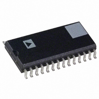
AD7874ARZ Analog Devices Inc, AD7874ARZ Datasheet - Page 7

AD7874ARZ
Manufacturer Part Number
AD7874ARZ
Description
IC DAS 12BIT 4CH 5V 28-SOIC
Manufacturer
Analog Devices Inc
Type
Data Acquisition System (DAS)r
Datasheet
1.AD7874ARZ.pdf
(16 pages)
Specifications of AD7874ARZ
Resolution (bits)
12 b
Data Interface
Parallel
Sampling Rate (per Second)
116k
Voltage Supply Source
Dual ±
Voltage - Supply
5V
Operating Temperature
-40°C ~ 85°C
Mounting Type
Surface Mount
Package / Case
28-SOIC (7.5mm Width)
Sampling Rate
116kSPS
Input Channel Type
Single Ended
Supply Voltage Range - Analog
± 4.75V To ± 5.25V
Supply Current
12mA
Lead Free Status / RoHS Status
Lead free / RoHS Compliant
Available stocks
Company
Part Number
Manufacturer
Quantity
Price
Part Number:
AD7874ARZ
Manufacturer:
ADI/亚德诺
Quantity:
20 000
Company:
Part Number:
AD7874ARZ-REEL
Manufacturer:
SANKEN
Quantity:
1 202
REV. C
OFFSET AND FULL-SCALE ADJUSTMENT
In most Digital Signal Processing (DSP) applications, offset and
full-scale errors have little or no effect on system performance.
Offset error can always be eliminated in the analog domain by
ac coupling. Full-scale error effect is linear and does not cause
problems as long as the input signal is within the full dynamic
range of the ADC. Invariably, some applications will require
that the input signal span the full analog input dynamic range.
In such applications, offset and full-scale error will have to be
adjusted to zero.
Figure 6 shows a circuit which can be used to adjust the offset
and full-scale errors on the AD7874 (Channel 1 is shown for ex-
ample purposes only). Where adjustment is required, offset er-
ror must be adjusted before full-scale error. This is achieved by
trimming the offset of the op amp driving the analog input of
the AD7874 while the input voltage is a 1/2 LSB below analog
ground. The trim procedure is as follows: apply a voltage of
–2.44 mV (–1/2 LSB) at V
offset voltage until the ADC output code flickers between 1111
1111 1111 and 0000 0000 0000.
011...110
000...010
111...110
011...111
000...001
000...000
111...111
100...001
100...000
Figure 6. AD7874 Full-Scale Adjust Circuit
Figure 5. Input/Output Transfer Function
10k
500
10k
INPUT
RANGE = 10V
R1
R2
R3
OUTPUT
CODE
V
1
*ADDITIONAL PINS OMITTED FOR CLARITY
–
FS
2
R5
10k
1
10k
R4
in Figure 6 and adjust the op amp
INPUT VOLTAGE
0V
V
AGND
IN1
AD7874*
1LSB =
FS=20V
+
FS
4096
2
FS
–
1LSB
–7–
Gain error can be adjusted at either the first code transition
(ADC negative full scale) or the last code transition (ADC posi-
tive full scale). The trim procedures for both cases are as
follows:
Positive Full-Scale Adjust
Apply a voltage of +9.9927 V (FS/2 – 3/2 LSBs) at V
R2 until the ADC output code flickers between 0111 1111 1110
and 0111 1111 1111.
Negative Full-Scale Adjust
Apply a voltage of –9.9976 V ( –FS + 1/2 LSB) at V
R2 until the ADC output code flickers between 1000 0000 0000
and 1000 0000 0001.
An alternative scheme for adjusting full-scale error in systems
which use an external reference is to adjust the voltage at the
REF IN pin until the full-scale error for any of the channels is
adjusted out. The good full-scale matching of the channels will
ensure small full-scale errors on the other channels.
TIMING AND CONTROL
Conversion is initiated on the AD7874 by asserting the
CONVST input. This CONVST input is an asynchronous input
which is independent of the ADC clock. This is essential for
applications where precise sampling in time is important. In
these applications, the signal sampling must occur at exactly
equal intervals to minimize errors due to sampling uncertainty
or jitter. In these cases, the CONVST input is driven from a
timer or precise clock source. Once conversion is started,
CONVST should not be asserted again until conversion is com-
plete on all four channels.
In applications where precise time interval sampling is not criti-
cal, the CONVST pulse can be generated from a microproces-
sor WRITE or READ line gated with a decoded address
(different to the AD7874 CS address). CONVST should not be
derived from a decoded address alone because very short
CONVST pulses (which may occur in some microprocessor sys-
tems as the address bus is changing at the start of an instruction
cycle) could initiate a conversion.
All four track/hold amplifiers go from track to hold on the rising
edge of the CONVST pulse. The four track/hold amplifiers re-
main in their hold mode while all four channels are converted.
The rising edge of CONVST also initiates a conversion on the
Channel 1 input voltage (V
on Channel 1, its result is stored in Data Register 1, one of four
on-chip registers used to store the conversion results. When the
result from the first conversion is stored, conversion is initiated
on the voltage held by track/hold 2. When conversion has been
completed on the voltage held by track/hold 4 and its result is
stored in Data Register 4, INT goes low to indicate that the
conversion process is complete.
The sequence in which the channel conversions takes place is
automatically taken care of by the AD7874. This means that the
user does not have to provide address lines to the AD7874 or
worry about selecting which channel is to be digitized.
Reading data from the device consists of four read operations to
the same microprocessor address. Addressing of the four
on-chip data registers is again automatically taken care of by the
AD7874.
IN1
). When conversion is complete
AD7874
1
1
and adjust
. Adjust


