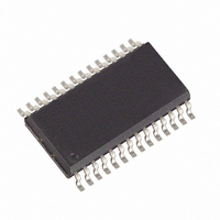
MAX196BCWI+ Maxim Integrated Products, MAX196BCWI+ Datasheet - Page 10

MAX196BCWI+
Manufacturer Part Number
MAX196BCWI+
Description
IC DAS 12BIT 6CH 28-SOIC
Manufacturer
Maxim Integrated Products
Type
Data Acquisition System (DAS)r
Datasheet
1.MAX196BCAI.pdf
(16 pages)
Specifications of MAX196BCWI+
Resolution (bits)
12 b
Sampling Rate (per Second)
100k
Data Interface
Parallel
Voltage Supply Source
Single Supply
Voltage - Supply
4.75 V ~ 5.25 V
Operating Temperature
0°C ~ 70°C
Mounting Type
Surface Mount
Package / Case
28-SOIC (7.5mm Width)
Lead Free Status / RoHS Status
Lead free / RoHS Compliant
The control byte is latched into the device, on pins
D7–D0, during a write cycle. Table 2 shows the control-
byte format.
The output data format is binary in unipolar mode and
twos-complement binary in bipolar mode. When reading
the output data, CS and RD must be low.
Conversions are initiated with a write operation, which
selects the mux channel and configures the MAX196/
MAX198 for either a unipolar or bipolar input range. A
write pulse (WR + CS) can either start an acquisition inter-
val or initiate a combined acquisition plus conversion. The
sampling interval occurs at the end of the acquisition
interval. The ACQMOD bit in the input control byte offers
two options for acquiring the signal: internal or external.
The conversion period lasts for 12 clock cycles in either
internal or external clock or acquisition mode.
Writing a new control byte during a conversion cycle will
abort the conversion and start a new acquisition interval.
Select internal acquisition by writing the control byte with
the ACQMOD bit cleared (ACQMOD = 0). This causes
the write pulse to initiate an acquisition interval whose
Multirange, Single +5V, 12-Bit DAS
with 12-Bit Bus Interface
Figure 5. Conversion Timing Using Internal Acquisition Mode
10
______________________________________________________________________________________
CS
WR
D7–D0
RD
INT
DOUT
t
CSWS
How to Start a Conversion
HIGH-Z
t
DS
t
WR
t
CS
ACQMOD ="0"
CONTROL
BYTE
Output Data Format
Internal Acquisition
t
ACQI
t
t
DH
CSWH
Input Format
t
CONV
t
D0
t
CSRS
duration is internally timed. Conversion starts when this
six-clock-cycle acquisition interval (3µs with f
2MHz) ends (see Figure 5).
Use the external acquisition timing mode for precise con-
trol of the sampling aperture and/or independent control
of acquisition and conversion times. The user controls
acquisition and start-of-conversion with two separate
write pulses. The first pulse, written with ACQMOD = 1,
starts an acquisition interval of indeterminate length. The
second write pulse, written with ACQMOD = 0, termi-
nates acquisition and starts conversion on WR’s rising
edge (Figure 6). However, if the second control byte
contains ACQMOD = 1, an indefinite acquisition interval
is restarted.
The address bits for the input mux must have the same
values on the first and second write pulses. Power-down
mode bits (PD0, PD1) can assume new values on the
second write pulse (see Power-Down Mode section).
A standard interrupt signal, INT, is provided to allow the
device to flag the µP when the conversion has ended
and a valid result is available. INT goes low when con-
version is complete and the output data is ready
(Figures 5 and 6). It returns high on the first read cycle
or if a new control byte is written.
t
INT1
DATA VALID
How to Read a Conversion
External Acquisition
t
t
CSRH
TR
HIGH-Z
CLK
=


