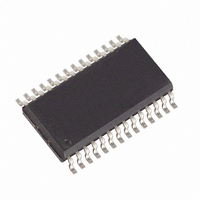
MAX196BCWI+ Maxim Integrated Products, MAX196BCWI+ Datasheet - Page 7

MAX196BCWI+
Manufacturer Part Number
MAX196BCWI+
Description
IC DAS 12BIT 6CH 28-SOIC
Manufacturer
Maxim Integrated Products
Type
Data Acquisition System (DAS)r
Datasheet
1.MAX196BCAI.pdf
(16 pages)
Specifications of MAX196BCWI+
Resolution (bits)
12 b
Sampling Rate (per Second)
100k
Data Interface
Parallel
Voltage Supply Source
Single Supply
Voltage - Supply
4.75 V ~ 5.25 V
Operating Temperature
0°C ~ 70°C
Mounting Type
Surface Mount
Package / Case
28-SOIC (7.5mm Width)
Lead Free Status / RoHS Status
Lead free / RoHS Compliant
Figure 1. Reference-Adjust Circuit
Figure 2. Load Circuits for Enable Time
______________________________________________________________Pin Description
16–21
3–14
PIN
15
22
23
24
25
26
27
28
D
1
2
OUT
a) High-Z to V
100k
24k
+5V
3k
CH0–CH5
REFADJ
D11–D0
NAME
AGND
DGND
REF
CLK
V
INT
WR
RD
CS
DD
OH
and V
510k
OL
_______________________________________________________________________________________
to V
0.01 F
Clock Input. In external clock mode, drive CLK with a TTL/CMOS-compatible clock. In internal clock mode,
place a capacitor (C
with C
Chip Select, active low
Three-State Digital I/O, D11 = MSB
Analog Ground
Analog Input Channels
Bandgap Voltage-Reference Output/External Adjust Pin. Bypass with a 0.01µF capacitor to AGND. Connect
to V
Reference Buffer Output/ADC Reference Input. In internal reference mode, the reference buffer provides a
4.096V nominal output, externally adjustable at REFADJ. In external reference mode, disable the internal
buffer by pulling REFADJ to V
INT goes low when conversion is complete and output data is ready.
If CS is low, a falling edge on RD will enable a read operation on the data bus.
In the internal acquisition mode, when CS is low, a rising edge on WR latches in configuration data and starts an
acquisition plus a conversion cycle. In the external acquisition mode, when CSis low, the first rising edge on WR
starts an acquisition, and a second rising edge on WR ends acquisition and starts a conversion cycle.
+5V Supply. Bypass with 0.1µF capacitor to AGND.
Digital Ground
C
LOAD
OH
DD
CLK
when using an external reference at the REF pin.
= 100pF.
b) High-Z to V
Multirange, Single +5V, 12-Bit DAS
REFADJ
D
OUT
MAX196
MAX198
CLK
3k
OL
) from this pin to ground to set the internal clock frequency; f
+5V
and V
C
LOAD
OH
DD
to V
.
OL
with 12-Bit Bus Interface
The MAX196/MAX198 multirange, fault-tolerant ADCs
use successive approximation and internal input
track/hold (T/H) circuitry to convert an analog signal to
a 12-bit digital output. The 12-bit parallel-output format
provides easy interface to microprocessors (µPs).
Figure 3 shows the MAX196/MAX198 in the simplest
operational configuration.
In the internal acquisition control mode (control bit D5
set to 0), the T/H enters its tracking mode on WR’s ris-
ing edge, and enters its hold mode when the internally
timed (6 clock cycles) acquisition interval ends. In bipo-
lar mode and unipolar mode (MAX196 only), a low-
impedance input source, which settles in less than
1.5µs, is required to maintain conversion accuracy at
the maximum conversion rate.
When the MAX198 is configured for unipolar mode, the
input does not need to be driven from a low-impedance
source. The acquisition time (t
source output resistance (R
tance (R
_______________Detailed Description
FUNCTION
IN
), and the T/H capacitance.
Analog-Input Track/Hold
S
Converter Operation
), the channel input resis-
AZ
CLK
) is a function of the
= 1.56MHz typical
7


