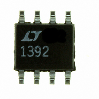
LTC1392CS8 Linear Technology, LTC1392CS8 Datasheet - Page 6

LTC1392CS8
Manufacturer Part Number
LTC1392CS8
Description
IC DATA ACQ SYSTEM 10BIT 8-SOIC
Manufacturer
Linear Technology
Type
Data Acquisition System (DAS)r
Datasheet
1.LTC1392CN8PBF.pdf
(12 pages)
Specifications of LTC1392CS8
Resolution (bits)
10 b
Sampling Rate (per Second)
25k
Data Interface
Serial
Voltage Supply Source
Single Supply
Voltage - Supply
4.5 V ~ 6 V
Operating Temperature
0°C ~ 70°C
Mounting Type
Surface Mount
Package / Case
8-SOIC (3.9mm Width)
Lead Free Status / RoHS Status
Contains lead / RoHS non-compliant
Available stocks
Company
Part Number
Manufacturer
Quantity
Price
Company:
Part Number:
LTC1392CS8
Manufacturer:
LNEAR
Quantity:
10 000
Company:
Part Number:
LTC1392CS8
Manufacturer:
LT
Quantity:
10 000
Part Number:
LTC1392CS8
Manufacturer:
LINEAR/凌特
Quantity:
20 000
Part Number:
LTC1392CS8#PBF
Manufacturer:
LINEAR/凌特
Quantity:
20 000
Company:
Part Number:
LTC1392CS8#TR
Manufacturer:
LINEAR
Quantity:
4 702
Company:
Part Number:
LTC1392CS8#TRPBF
Manufacturer:
LINEAR
Quantity:
6 567
APPLICATIONS
LTC1392
The LTC1392 is a micropower data acquisition system
designed to measure temperature, an on-chip power
supply voltage and a differential input voltage. The LTC1392
contains the following functional blocks:
1. On-chip temperature sensor
2. 10-bit successive approximation capacitive ADC
3. Bandgap reference
4. Analog multiplexer (MUX)
5. Sample-and-hold (S/H)
6. Synchronous, half-duplex serial interface
7. Control and timing logic
6
TEST CIRCUITS
Voltage Waveforms for D
D
OUT
D
OUT
t
r
TEST POINT
Load Circuit for t
D
Load Circuit for t
OUT
100pF
U
3k
INFORMATION
OUT
U
1.4V
Rise and Fall Times, t
3k
dDO
100pF
dis
, t
and t
r
W
and t
5V t
t
dis
en
TEST POINT
dis
WAVEFORM 1
LTC1392 • TC02
f
WAVEFORM 2, t
t
f
U
LTC1392 • TC05
r
and t
1392 TC04
en
V
V
OH
OL
f
DIGITAL CONSIDERATIONS
Serial Interface
The LTC1392 communicates with microprocessors and
other external circuitry via a synchronous, half-duplex,
3-wire serial interface (see Figure 1). The clock (CLK)
synchronizes the data transfer with each bit being trans-
mitted on the falling CLK edge and captured on the rising
CLK edge in both transmitting and receiving systems. The
input data is first received and then the A/D conversion
result is transmitted (half-duplex). Half-duplex operation
allows D
sion over three wires: CS, CLK and DATA (D
transfer is initiated by a falling chip select (CS) signal. After
the falling CS is recognized, an 80 s delay is needed for
WAVEFORM 1
WAVEFORM 2
(SEE NOTE 1)
(SEE NOTE 2)
D
CLK
OUT
D
D
OUT
OUT
Voltage Waveforms for D
IN
CS
and D
NOTE 1: WAVEFORM 1 IS FOR AN OUTPUT WITH INTERNAL CONDITIONS SUCH
THAT THE OUTPUT IS HIGH UNTIL DISABLED BY THE OUTPUT CONTROL.
NOTE 2: WAVEFORM 2 IS FOR AN OUTPUT WITH INTERNAL CONDITIONS SUCH
THAT THE OUTPUT IS LOW UNTIL DISABLED BY THE OUTPUT CONTROL.
OUT
Voltage Waveforms for t
V
IL
to be tied together allowing transmis-
t
dDO
OUT
Delay Time, t
t
dis
dis
LTC1392 • TC03
IN
2.0V
/D
dDO
OUT
10%
90%
V
V
LTC1392 • TC06
). Data
OH
OL


