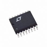
LTC1293CCSW#TR Linear Technology, LTC1293CCSW#TR Datasheet - Page 15

LTC1293CCSW#TR
Manufacturer Part Number
LTC1293CCSW#TR
Description
IC DATA ACQ SYS 12BIT 5V 16SOIC
Manufacturer
Linear Technology
Type
Data Acquisition System (DAS), ADCr
Datasheet
1.LTC1296CCSWPBF.pdf
(28 pages)
Specifications of LTC1293CCSW#TR
Resolution (bits)
12 b
Sampling Rate (per Second)
46.5k
Data Interface
Serial, Parallel
Voltage Supply Source
Dual ±
Voltage - Supply
±5V
Operating Temperature
0°C ~ 70°C
Mounting Type
Surface Mount
Package / Case
16-SOIC (0.300", 7.5mm Width)
Lead Free Status / RoHS Status
Contains lead / RoHS non-compliant
D
Motorola SPI (MC68HC11)
The MC68HC11 has been chosen as an example of an MPU
with a dedicated serial port. This MPU transfers data MSB-
first and in 8-bit increments. The D
register starts the SPI process. With three 8-bit transfers,
the A/D result is read into the MPU. The second 8-bit
transfer clocks B11 through B8 of the A/D conversion
result into the processor. The third 8-bit transfer clocks
the remaining bits B7 through B0 into the MPU. The data
is right justified in the two memory locations. ANDing the
second byte with 0D
bits. This operation was not included in the code. It can
be inserted in the data gathering loop or outside the loop
when the data is processed.
CLK
A
OUT
CS
D
IN
TRANSMIT
RECEIVED
PPLICATI
WORD
WORD
MPU
MPU
#62
#63
0
?
0
?
O
B7
D OUT FROM LTC1294 STORED ON MC68HC11 RAM
O
0
?
START
U
O
B6
HEX
BYTE 1
BYTE 1
START
S
1
?
SGL/
DIFF
clears the four most significant
O
B5
SGL
I FOR ATIO
?
U
ODD/
EVEN
ODD
B4
?
O
SEL
SEL
1
MSB
1
?
IN
B11
Hardware and Software Interface to Motorola MC68HC11
B3
word sent to the data
W
SEL
SEL
0
0
?
Data Exchange Between LTC1294 and MC68HC11
B10
B2
UNI
B1
B9
UNI MSBF
?
U
MSBF
LSB
B8
B0
?
BYTE 1
BYTE 2
PS
PS
?
X
0
BYTE 2
BYTE 2
ANALOG
B11
INPUTS
Interfacing to the Parallel Port of the Intel 8051 Family
The Intel 8051 has been chosen to show the interface
between the LTC1293/4/6 and parallel port microproces-
sors. Usually the signals CS, D
on three port lines and the D
port line. This works very well. One can save a line by tying
the D
start bit and D
P1.2. Then P1.2 is reconfigured as an input and the 8051
reads back the 12-bit A/D result over the same data line.
B11
X
B10
B10
IN
X
and D
B9
LTC1293/LTC1294/LTC1296
B9
X
B8
B8
X
LTC1294
OUT
IN
to the LTC1294 over the line connected to
lines together. The 8051 first sends the
B7
D
CLK
OUT
D
CS
IN
DON'T CARE
B7
X
B6
B6
X
OUT
B5
B5
X
IN
BYTE 3 (DUMMY)
B4
signal is read on a fourth
B4
and CLK are generated
X
DO
SCK
MOSI
MISO
BYTE 3
B3
B3
MC68HC11
X
B2
B2
X
B1
B1
X
LTC1293 TD01a
B0
B0
X
15
129346fs
LTC1293 TD01


