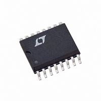
LTC1293CCSW#TR Linear Technology, LTC1293CCSW#TR Datasheet - Page 23

LTC1293CCSW#TR
Manufacturer Part Number
LTC1293CCSW#TR
Description
IC DATA ACQ SYS 12BIT 5V 16SOIC
Manufacturer
Linear Technology
Type
Data Acquisition System (DAS), ADCr
Datasheet
1.LTC1296CCSWPBF.pdf
(28 pages)
Specifications of LTC1293CCSW#TR
Resolution (bits)
12 b
Sampling Rate (per Second)
46.5k
Data Interface
Serial, Parallel
Voltage Supply Source
Dual ±
Voltage - Supply
±5V
Operating Temperature
0°C ~ 70°C
Mounting Type
Surface Mount
Package / Case
16-SOIC (0.300", 7.5mm Width)
Lead Free Status / RoHS Status
Contains lead / RoHS non-compliant
A
PPLICATI
Figure 17. LTC1294 ENOB vs Input Frequency
–100
–120
–140
–100
–120
–140
10.0
12.0
11.5
11.0
10.5
–20
–40
–60
–80
–20
–40
–60
–80
9.5
9.0
8.5
8.0
0
0
0
0
0
Figure 16b. LTC1294 FFT Plot
f
SNR = 72.5dB with ±5V Supplies
Figure 16a. LTC1294 FFT Plot
f
SNR = 72.7dB with ±5V Supplies
IN
f
IN
S
O
= 45.4kHz
= 22kHz, f
= 1kHz, f
U
20
5
5
S
FREQUENCY (kHz)
FREQUENCY (kHz)
FREQUENCY (kHz)
40
S
I FOR ATIO
10
10
S
U
±5V SUPPLIES
= 45.4kHz,
= 45.4kHz,
+5V SUPPLY
60
15
15
W
80
20
20
LT1293 F17
1293 F16a
1293 F16b
100
25
25
U
For +5V supplies the ENOB decreases more rapidly. This
is due predominantly to the 2nd harmonic distortion term.
Figure 18 shows a FFT plot of the output spectrum for two
tones applied to the input of the A/D. Nonlinearities in the
A/D will cause distortion products at the sum and differ-
ence frequencies of the fundamentals and products of the
fundamentals. This is classically referred to as
intermodulation distortion (IMD).
Overvoltage Protection
Applying signals to the LTC1293/4/6’s analog inputs that
exceed the positive supply or that go below V
degrade the accuracy of the A/D and possibly damage the
device. For example this condition would occur if a signal
is applied to the analog inputs before power is applied to
the LTC1293/4/6. Another example is the input source is
operating from different supplies of larger value than the
LTC1293/4/6. These conditions should be prevented ei-
ther with proper supply sequencing or by use of external
circuitry to clamp or current limit the input source. There
are two ways to protect the inputs. In Figure 19 diode
clamps from the inputs to V
second method is to put resistors in series with the analog
inputs for current limiting. As shown in Figure 20a, a 1kΩ
resistor is enough to stand off ±15V (15mA for only one
channel). If more than one channel exceeds the supplies
than the following guidelines can be used. Limit the
current to 7mA per channel and 28mA for all channels.
LTC1293/LTC1294/LTC1296
–100
–120
–140
–20
–40
–60
–80
Figure 18. LTC1294 FFT Plot
f
with ±5V Supplies
0
IN
0
1 = 5.1kHz, f
5
FREQUENCY (kHz)
10
IN
2 = 5.6kHz, f
CC
15
and V
20
S
= 45.4kHz
–
1293 F8
are used. The
25
23
–
129346fs
will


