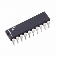
LTC1289BCN Linear Technology, LTC1289BCN Datasheet - Page 15

LTC1289BCN
Manufacturer Part Number
LTC1289BCN
Description
IC DATA ACQ SYS 12BIT 3V 20-DIP
Manufacturer
Linear Technology
Type
Data Acquisition System (DAS)r
Datasheet
1.LTC1289CCN.pdf
(28 pages)
Specifications of LTC1289BCN
Resolution (bits)
12 b
Sampling Rate (per Second)
25k
Data Interface
Serial, Parallel
Voltage Supply Source
Dual ±
Voltage - Supply
3V
Operating Temperature
0°C ~ 70°C
Mounting Type
Through Hole
Package / Case
20-DIP (0.300", 7.62mm)
Lead Free Status / RoHS Status
Contains lead / RoHS non-compliant
Available stocks
Company
Part Number
Manufacturer
Quantity
Price
Part Number:
LTC1289BCN#PBF
Manufacturer:
LINEAR/凌特
Quantity:
20 000
Logic Levels
The logic level standards for this supply range have not
been well defined. What standards that do exist are not
universally accepted. The trip point on the logic inputs of
the LTC1289 is 0.28 × V
compatible with HC type logic levels and processors that
are specified at 3.3V. The output D
with the above standards. The following summarizes such
levels.
The LTC1289 can be driven with 5V logic even when V
is at 3.3V. This is due to a unique input protection device
that is found on the LTC1289.
Microprocessor Interfaces
The LTC1289 can interface directly (without external hard-
ware) to most popular microprocessor (MPU) synchro-
nous serial formats. If an MPU without a serial interface is
used, then four of the MPU’s parallel port lines can be
programmed to form the serial link to the LTC1289. Many
of the popular MPU's can operate with 3V supplies. For
example the MC68HC11 is an MPU with a serial format
(SPI). Likewise parallel MPU’s that have the 8051 type
architecture are also capable of operating at this voltage
A
PPLICATI
V
V
OH
OL
(no load)
(no load)
V
V
V
V
OH
OL
IH
IL
O
U
S
CC
I FOR ATIO
U
. This makes the logic inputs
Figure 5. Several LTC1289s Sharing One 3-Wire Serial Interface
OUT
OUTPUT PORT
2
V
W
0.9 × V
0.1 × V
0.7 × V
0.2 × V
SERIAL DATA
CC
MPU
is also compatible
1
0.1V
- 0.1V
0
CC
CC
CC
CC
U
3
3
8 CHANNELS
LTC1289
CC
CS
range. The code for these processors remains the same
and can be found in the LTC1290 datasheet or application
notes AN36A and AN36B.
Sharing the Serial Interface
The LTC1289 can share 3-wire serial interface with other
peripheral components or other LTC1289s (See Figure 5).
In this case, the CS signals decide which LTC1289 is being
addressed by the MPU.
ANALOG CONSIDERATIONS
1. Grounding
The LTC1289 should be used with an analog ground plane
and single point grounding techniques.
Pin 11 (AGND) should be tied directly to this ground plane.
Pin 10 (DGND) can also be tied directly to this ground
plane because minimal digital noise is generated within
the chip itself.
Pin 20 (V
22µF tantalum with leads as short as possible. Pin 12 (V
should be bypassed with a 0.1µF ceramic disk. For single
supply applications, V
It is also recommended that pin 13 (REF
be tied directly to the ground plane. All analog inputs
should be referenced directly to the single point ground.
Digital inputs and outputs should be shielded from and/or
routed away from the reference and analog circuitry.
3
8 CHANNELS
LTC1289
CC
CS
) should be bypassed to the ground plane with a
3
8 CHANNELS
LTC1289
CS
–
can be tied to the ground plane.
3-WIRE SERIAL
INTERFACE TO OTHER
PERIPHERALS OR LTC1289s
–
) and pin 9 (COM)
LTC1289 AIF05
LTC1289
15
1289fb
–
)


