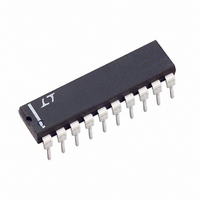
LTC1289BCN Linear Technology, LTC1289BCN Datasheet - Page 17

LTC1289BCN
Manufacturer Part Number
LTC1289BCN
Description
IC DATA ACQ SYS 12BIT 3V 20-DIP
Manufacturer
Linear Technology
Type
Data Acquisition System (DAS)r
Datasheet
1.LTC1289CCN.pdf
(28 pages)
Specifications of LTC1289BCN
Resolution (bits)
12 b
Sampling Rate (per Second)
25k
Data Interface
Serial, Parallel
Voltage Supply Source
Dual ±
Voltage - Supply
3V
Operating Temperature
0°C ~ 70°C
Mounting Type
Through Hole
Package / Case
20-DIP (0.300", 7.62mm)
Lead Free Status / RoHS Status
Contains lead / RoHS non-compliant
Available stocks
Company
Part Number
Manufacturer
Quantity
Price
Part Number:
LTC1289BCN#PBF
Manufacturer:
LINEAR/凌特
Quantity:
20 000
3. Analog Inputs
Because of the capacitive redistribution A/D conversion
techniques used, the analog inputs of the LTC1289 have
capacitive switching input current spikes. These current
spikes settle quickly and do not cause a problem. How-
ever, if large source resistances are used or if slow settling
op amps drive the inputs, care must be taken to insure that
the transients caused by the current spikes settle com-
pletely before the conversion begins.
Source Resistance
The analog inputs of the LTC1289 look like a 100pF
capacitor (C
shown in Figure 9. This value for R
With larger supply voltages R
example with V
500Ω. C
inputs once during each conversion cycle. Large external
source resistors and capacitances will slow the settling of
A
PPLICATI
V
V
“+” INPUT
“–” INPUT
IN
IN
–
+
IN
ACLK
SCLK
CS
Figure 9. Analog Input Equivalent Circuit
gets switched between the selected “+” and “–”
R
R
IN
SOURCE
SOURCE
) is series with a 1500Ω resistor (R
CC
O
+
–
= 2.7V and V
1
U
C1
INPUT
INPUT
C2
S
“+”
“–”
MUX ADDRESS
SHIFTED IN
I FOR ATIO
2
U
ON
–
3
= – 2.7V R
4TH SCLK
LAST SCLK
will be reduced. For
ON
W
R
Figure 10. “+” and “–” Input Settling Windows
is for V
ON
SAMPLE
4
= 1.5k
ON
LTC1289
CC
DURING THIS TIME
C
100pF
LTC1289 AIF09
• • •
• • •
• • •
becomes
IN
MUST SETTLE
U
=
“+” INPUT
= 2.7V.
ON
t
SMPL
) as
HOLD
the inputs. It is important that the overall RC time con-
stants be short enough to allow the analog inputs to
completely settle within the allotted time.
“+” Input Settling
This input capacitor is switched onto the “+” input during
the sample phase (t
phase starts at the 4th SCLK cycle and lasts until the falling
edge of the last SCLK (the 8th, 12th or 16th SCLK cycle
depending on the selected word length). The voltage on
the “+” input must settle completely within this sample
time. Minimizing R
settling time. If large “+” input source resistance must be
used, the sample time can be increased by using a slower
SCLK frequency or selecting a longer word length. With
the minimum possible sample time of 4µs, R
and C1 < 20pF will provide adequate settling.
“–” Input Settling
At the end of the sample phase the input capacitor switches
to the “–” input and the conversion starts (see Figure 10).
During the conversion, the “+” input voltage is effectively
“held” by the sample and hold and will not affect the
conversion result. However, it is critical that the “–” input
voltage be free of noise and settle completely during the
first four ACLK cycles of the conversion time. Minimizing
R
input source resistance must be used, the time allowed for
“–” INPUT MUST SETTLE
SOURCE
DURING THIS TIME
1
1ST BIT TEST
LAST SCLK (8TH, 12TH OR 16TH DEPENDING ON WORK LENGTH)
2
–
and C2 will improve settling time. If large “–”
3
4
SOURCE
SMPL
+
, see Figure 10). The sample
and C1 will improve the input
• • •
LTC1289
SOURCE
1289 AIF10
17
+
< 2k
1289fb


