LM12H458CIVF/NOPB National Semiconductor, LM12H458CIVF/NOPB Datasheet - Page 8
LM12H458CIVF/NOPB
Manufacturer Part Number
LM12H458CIVF/NOPB
Description
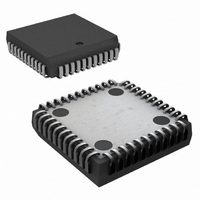
IC ACQUISITION SYS 12BIT 44-PLCC
Manufacturer
National Semiconductor
Type
Data Acquisition System (DAS)r
Datasheet
1.LM12458CIVNOPB.pdf
(36 pages)
Specifications of LM12H458CIVF/NOPB
Resolution (bits)
12 b
Sampling Rate (per Second)
140k
Data Interface
Parallel
Voltage Supply Source
Analog and Digital
Voltage - Supply
3 V ~ 5.5 V
Operating Temperature
-40°C ~ 85°C
Mounting Type
Surface Mount
Package / Case
44-PLCC
Lead Free Status / RoHS Status
Lead free / RoHS Compliant
Other names
*LM12H458CIVF
*LM12H458CIVF/NOPB
LM12H458CIVF
*LM12H458CIVF/NOPB
LM12H458CIVF
Available stocks
Company
Part Number
Manufacturer
Quantity
Price
Company:

Part Number:
LM12H458CIVF/NOPB
Manufacturer:
Texas Instruments
Quantity:
10 000


www.national.com
V
V
I
I
C
V
V
I
IN(1)
IN(0)
OUT
Symbol (See Figures
Digital Characteristics
The following specifications apply to the LM12454, LM12458, and LM12H458 for V
Boldface limits apply for T
IN(1)
IN(0)
OUT(1)
OUT(0)
Digital Timing Characteristics
The following specifications apply to the LM12454, LM12458, and LM12H458 for V
pF on data I/O, INT and DMARQ lines unless otherwise specified. Boldface limits apply for T
limits T
IN
Symbol
8, 9, 10)
A
1, 3
2, 4
= T
10
11
12
13
14
15
16
17
18
20
21
19
22
23
5
6
7
8
9
J
Logical “1” Input Voltage
Logical “0” Input Voltage
Logical “1” Input Current
Logical “0” Input Current
D0–D15 Input Capacitance
Logical “1” Output Voltage
Logical “0” Output Voltage
TRI-STATE
= 25˚C.
®
CS or Address Valid to ALE Low Set-Up
Time
CS or Address Valid to ALE Low Hold
Time
ALE Pulse Width
RD High to Next ALE High
ALE Low to RD Low
RD Pulse Width
RD High to Next RD or WR Low
ALE Low to WR Low
WR Pulse Width
WR High to Next ALE High
WR High to Next RD or WR Low
Data Valid to WR High Set-Up Time
Data Valid to WR High Hold Time
RD Low to Data Bus Out of TRI-STATE
RD High to TRI-STATE
RD Low to Data Valid (Access Time)
Address Valid or CS Low to RD Low
Address Valid or CS Low to WR Low
Address Invalid from RD or WR High
INT High from RD Low
DMARQ Low from RD Low
Output Leakage Current
Parameter
A
= T
J
= T
(Notes 6, 7)
MIN
Parameter
to T
MAX
(Notes 6, 7, 8)
; all other limits T
V
V
V
V
V
V
I
V
V
OUT
A
A
IN
IN
A
A
OUT
OUT
I
I
+ = V
+ = V
+ = V
+ = V
OUT
OUT
= 5V
= 0V
Conditions
= 1.6 mA
= 0V
= 5V
8
= −360 µA
= −10 µA
D
D
D
D
+ = 5.5V
+ = 4.5V
+ = 4.5V
+ = 4.5V
A
R
= T
Conditions
L
= 1 kΩ
J
= 25˚C.
A
A
(Note 10)
+ = V
Typical
+ = V
−0.005
0.005
−0.01
0.01
6
(Note 10)
Typical
D
D
+ = 5V, unless otherwise specified.
+ = 5V, t
40
30
30
30
30
A
= T
r
(Note 11)
J
= t
Limits
= T
−1.0
−3.0
4.25
(Note 11)
2.0
0.8
1.0
2.4
0.4
3.0
f
Limits
= 3 ns, and C
100
100
140
110
MIN
40
20
45
35
20
20
60
75
40
30
10
70
10
10
80
20
20
10
10
60
10
60
to T
MAX
µA (max)
µA (max)
µA (max)
µA (max)
V (max)
V (max)
V (min)
V (min)
V (min)
ns (max)
ns (max)
ns (max)
ns (max)
ns (max)
; all other
ns (min)
ns (min)
ns (min)
ns (min)
ns (min)
ns (min)
ns (min)
ns (min)
ns (min)
ns (min)
ns (min)
ns (min)
ns (min)
ns (min)
ns (min)
ns (min)
ns (min)
ns (min)
ns (min)
ns (min)
ns (min)
Units
L
Units
pF
= 100
Related parts for LM12H458CIVF/NOPB
Image
Part Number
Description
Manufacturer
Datasheet
Request
R

Part Number:
Description:
National Semiconductor [8-Bit D/A Converter]
Manufacturer:
National Semiconductor
Datasheet:
Part Number:
Description:
National Semiconductor [Media Coprocessor]
Manufacturer:
National Semiconductor
Datasheet:
Part Number:
Description:
Digitally Controlled Tone and Volume Circuit with Stereo Audio Power Amplifier, Microphone Preamp Stage and National 3D Sound
Manufacturer:
National Semiconductor
Datasheet:
Part Number:
Description:
Digitally Controlled Tone and Volume Circuit with Stereo Audio Power Amplifier, Microphone Preamp Stage and National 3D Sound
Manufacturer:
National Semiconductor
Datasheet:
Part Number:
Description:
AC97 Rev 2 Codec with Sample Rate Conversion and National 3D Sound
Manufacturer:
National Semiconductor
Part Number:
Description:
Manufacturer:
National Semiconductor
Datasheet:
Part Number:
Description:
Manufacturer:
National Semiconductor
Datasheet:
Part Number:
Description:
General Purpose, Low Voltage, Low Power, Rail-to-Rail Output Operational Amplifiers
Manufacturer:
National Semiconductor
Datasheet:
Part Number:
Description:
8-bit 20 MSPS flash A/D converter.
Manufacturer:
National Semiconductor
Datasheet:
Part Number:
Description:
Low Noise Quad Operational Amplifier
Manufacturer:
National Semiconductor
Datasheet:
Part Number:
Description:
Quad Differential Line Receivers
Manufacturer:
National Semiconductor
Datasheet:
Part Number:
Description:
Quad High Speed Trapezoidal? Bus Transceiver
Manufacturer:
National Semiconductor
Datasheet:
Part Number:
Description:
Dual Line Receiver
Manufacturer:
National Semiconductor
Datasheet:
Part Number:
Description:
TTL to 10k ECL Level Translator with Latch
Manufacturer:
National Semiconductor
Datasheet: