LM12H458CIVF/NOPB National Semiconductor, LM12H458CIVF/NOPB Datasheet - Page 9
LM12H458CIVF/NOPB
Manufacturer Part Number
LM12H458CIVF/NOPB
Description
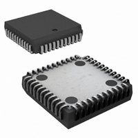
IC ACQUISITION SYS 12BIT 44-PLCC
Manufacturer
National Semiconductor
Type
Data Acquisition System (DAS)r
Datasheet
1.LM12458CIVNOPB.pdf
(36 pages)
Specifications of LM12H458CIVF/NOPB
Resolution (bits)
12 b
Sampling Rate (per Second)
140k
Data Interface
Parallel
Voltage Supply Source
Analog and Digital
Voltage - Supply
3 V ~ 5.5 V
Operating Temperature
-40°C ~ 85°C
Mounting Type
Surface Mount
Package / Case
44-PLCC
Lead Free Status / RoHS Status
Lead free / RoHS Compliant
Other names
*LM12H458CIVF
*LM12H458CIVF/NOPB
LM12H458CIVF
*LM12H458CIVF/NOPB
LM12H458CIVF
Available stocks
Company
Part Number
Manufacturer
Quantity
Price
Company:

Part Number:
LM12H458CIVF/NOPB
Manufacturer:
Texas Instruments
Quantity:
10 000


Digital Timing Characteristics
Note 1: Absolute Maximum Ratings indicate limits beyond which damage to the device may occur. Operating Ratings indicate conditions for which the device is
functional, but do not guarantee specific performance limits. For guaranteed specifications and test conditions, see the Electrical Characteristics. The guaranteed
specifications apply only for the test conditions listed. Some performance characteristics may degrade when the device is not operated under the listed test
conditions.
Note 2: All voltages are measured with respect to GND, unless otherwise specified.
Note 3: When the input voltage (V
The 20 mA maximum package input current rating allows the voltage at any four pins, with an input current of 5 mA, to simultaneously exceed the power supply
voltages.
Note 4: The maximum power dissipation must be derated at elevated temperatures and is dictated by T
to ambient thermal resistance), and T
Note 5: Human body model, 100 pF discharged through a 1.5 kΩ resistor.
Note 6: Two on-chip diodes are tied to each analog input through a series resistor, as shown below. Input voltage magnitude up to 5V above V
will not damage the LM12454 or the LM12(H)458. However, errors in the A/D conversion can occur if these diodes are forward biased by more than 100 mV. As an
example, if V
Note 7: V
conversion/comparison accuracy.
Note 8: Accuracy is guaranteed when operating at f
Note 9: With the test condition for V
Note 10: Typical figures are at T
Note 11: Limits are guaranteed to National’s AOQL (Average Output Quality Level).
Note 12: Positive integral linearity error is defined as the deviation of the analog value, expressed in LSBs, from the straight line that passes through positive
full-scale and zero. For negative integral linearity error the straight line passes through negative full-scale and zero. (See Figure 6 Figure 7).
Note 13: Zero error is a measure of the deviation from the mid-scale voltage (a code of zero), expressed in LSB. It is the worst-case value of the code transitions
between −1 to 0 and 0 to +1 (see Figure 8).
Note 14: The DC common-mode error is measured with both inputs shorted together and driven from 0V to 5V. The measured value is referred to the resulting
output value when the inputs are driven with a 2.5V signal.
Note 15: Power Supply Sensitivity is measured after Auto-Zero and/or Auto-Calibration cycle has been completed with V
Note 16: V
Note 17: The LM12(H)454/8’s self-calibration technique ensures linearity and offset errors as specified, but noise inherent in the self-calibration process will result
in a repeatability uncertainty of
Note 18: The Throughput Rate is for a single instruction repeated continuously. Sequencer states 0 (1 clock cycle), 1 (1 clock cycle), 7 (9 clock cycles) and 5 (44
clock cycles) are used (see Figure 15). One additional clock cycle is used to read the conversion result stored in the FIFO, for a total of 56 clock cycles per
conversion. The Throughput Rate is f
A
+ and V
REFCM
A
+ is 4.5 V
(Reference Voltage Common Mode Range) is defined as (V
D
+ must be connected together to the same power supply voltage and bypassed with separate capacitors at each V
DC
, full-scale input voltage must be ≤4.6 V
±
A
0.10 LSB.
IN
= 25˚C and represent most likely parametric norm.
) at any pin exceeds the power supply rails (V
REF
CLK
A
(ambient temperature).
(V
(MHz)/N, where N is the number of clock cycles/conversion.
REF+
− V
CLK
REF−
= 5 MHz for the LM12454/8 and f
) given as +5V, the 12-bit LSB is 1.22 mV and the 8-bit/“Watchdog” LSB is 19.53 mV.
(Notes 6, 7, 8) (Continued)
DC
to ensure accurate conversions.
REF+
9
IN
<
+ V
GND or V
REF−
CLK
)/2.
IN
= 8 MHz for the LM12H458.
>
01126403
(V
Jmax
A
+ or V
(maximum junction temperature), θ
D
+)), the current at that pin should be limited to 5 mA.
A
+ and V
D
+ at the specified extremes.
A
JA
+ or 5V below GND
(package junction
+
www.national.com
pin to assure
Related parts for LM12H458CIVF/NOPB
Image
Part Number
Description
Manufacturer
Datasheet
Request
R

Part Number:
Description:
National Semiconductor [8-Bit D/A Converter]
Manufacturer:
National Semiconductor
Datasheet:
Part Number:
Description:
National Semiconductor [Media Coprocessor]
Manufacturer:
National Semiconductor
Datasheet:
Part Number:
Description:
Digitally Controlled Tone and Volume Circuit with Stereo Audio Power Amplifier, Microphone Preamp Stage and National 3D Sound
Manufacturer:
National Semiconductor
Datasheet:
Part Number:
Description:
Digitally Controlled Tone and Volume Circuit with Stereo Audio Power Amplifier, Microphone Preamp Stage and National 3D Sound
Manufacturer:
National Semiconductor
Datasheet:
Part Number:
Description:
AC97 Rev 2 Codec with Sample Rate Conversion and National 3D Sound
Manufacturer:
National Semiconductor
Part Number:
Description:
Manufacturer:
National Semiconductor
Datasheet:
Part Number:
Description:
Manufacturer:
National Semiconductor
Datasheet:
Part Number:
Description:
General Purpose, Low Voltage, Low Power, Rail-to-Rail Output Operational Amplifiers
Manufacturer:
National Semiconductor
Datasheet:
Part Number:
Description:
8-bit 20 MSPS flash A/D converter.
Manufacturer:
National Semiconductor
Datasheet:
Part Number:
Description:
Low Noise Quad Operational Amplifier
Manufacturer:
National Semiconductor
Datasheet:
Part Number:
Description:
Quad Differential Line Receivers
Manufacturer:
National Semiconductor
Datasheet:
Part Number:
Description:
Quad High Speed Trapezoidal? Bus Transceiver
Manufacturer:
National Semiconductor
Datasheet:
Part Number:
Description:
Dual Line Receiver
Manufacturer:
National Semiconductor
Datasheet:
Part Number:
Description:
TTL to 10k ECL Level Translator with Latch
Manufacturer:
National Semiconductor
Datasheet: