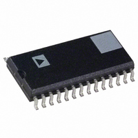
AD7729AR Analog Devices Inc, AD7729AR Datasheet - Page 4

AD7729AR
Manufacturer Part Number
AD7729AR
Description
IC ADC 15BIT DUAL W/DAC 28-SOIC
Manufacturer
Analog Devices Inc
Type
ADC, DACr
Datasheet
1.AD7729ARUZ-REEL.pdf
(16 pages)
Specifications of AD7729AR
Rohs Status
RoHS non-compliant
Resolution (bits)
15 b
Sampling Rate (per Second)
270.8k
Data Interface
Serial
Voltage Supply Source
Analog and Digital
Voltage - Supply
3V
Operating Temperature
-40°C ~ 105°C
Mounting Type
Surface Mount
Package / Case
28-SOIC (7.5mm Width)
Available stocks
Company
Part Number
Manufacturer
Quantity
Price
Company:
Part Number:
AD7729ARU
Manufacturer:
LT
Quantity:
5 460
Part Number:
AD7729ARU
Manufacturer:
ADI/亚德诺
Quantity:
20 000
Company:
Part Number:
AD7729ARUREEL
Manufacturer:
AD
Quantity:
7 066
Part Number:
AD7729ARUZ
Manufacturer:
ADI/亚德诺
Quantity:
20 000
Company:
Part Number:
AD7729ARUZREEL7
Manufacturer:
VISHAY
Quantity:
2 776
Part Number:
AD7729ARZ
Manufacturer:
ADI/亚德诺
Quantity:
20 000
Company:
Part Number:
AD7729ARZ-RL
Manufacturer:
NXP
Quantity:
36 000
AD7729
Baseband Section
V
V
ADC
TIMING CHARACTERISTICS
Parameter
AUXILIARY FUNCTIONS
Clock Signals
t
t
t
t
t
t
t
t
t
t
t
t
t
t
Receive Section
Clock Signals
t
t
t
t
t
t
t
t
t
t
t
ASCLK = MCLK/(2
BSCLK = MCLK/(2
Specifications subject to change without notice.
1
2
3
4
5
6
10
11
12
13
14
15
16
17
7
8
9
18
19
20
21
22
23
24
25
ADC Signal Range
V
Signal Range
REFCAP
REFOUT
BIAS
Differential Input
Single-Ended Input
Differential
Single-Ended
Table II. Receive Section Signal Ranges
ASCLKRATE). ASCLKRATE can have a value from 0 . . . 1023. When ASCLKRATE = 0, ASCLK = 13 MHz.
BSCLKRATE). BSCLKRATE can have a value from 0 . . . 1023. When BSCLKRATE = 0, BSCLK = 13 MHz.
Signal Range
1.3 V
1.3 V
2 V
V
V
V
V
REFCAP
REFCAP
BIAS
BIAS
REFCAP
Limit at
T
76
30.4
30.4
t
0.4
0.4
20
10
15
0
0
15
10
t
t
0.4
0.4
20
10
15
0
0
15
10
t
1
4
1
7
A
+ 15
+ 15
/2 to (AVDD1 – V
V
V
5%
10%
to (AVDD1 – V
= –40 C to +105 C
REFCAP
REFCAP
t
t
t
t
1
1
1
1
(AVDD1 = AVDD2 = +3 V
T
A
/2
= T
MIN
to T
REFCAP
MAX
REFCAP
, unless otherwise noted)
)
/2)
–4–
Units
ns min
ns min
ns min
ns min
ns min
ns min
ns min
ns min
ns max
ns min
ns min
ns max
ns min
ns min
ns min
ns min
ns min
ns min
ns min
ns max
ns min
ns min
ns max
ns min
ns min
10%; DVDD1 = DVDD2 = +3 V
AUXDAC
Output Code
Code 000
Code 3FF
Table III. Auxiliary Section Signal Ranges
See Figure 2.
MCLK Period
MCLK Width Low
MCLK Width High
ASCLK Period. See Figures 4 and 6.
ASCLK Width Low
ASCLK Width High
ASDI/ASDIFS Setup Before ASCLK Low
ASDI/ASDIFS Hold After ASCLK Low
ASDOFS Delay from ASCLK High
ASDOFS Hold After ASCLK High
ASDO Hold After ASCLK High
ASDO Delay from ASCLK High
ASDIFS Low to ASDI LSB Read by ASPORT
Interval Between Consecutive ASDIFS Pulses
See Figures 5 and 7.
BSCLK Period
BSCLK Width Low
BSCLK Width High
BSDI/BSDIFS Setup Before BSCLK Low
BSDI/BSDIFS HoldAfter BSCLK Low
BSDOFS Delay from BSCLK High
BSDOFS Hold After BSCLK High
BSDO Hold After BSCLK High
BSDO Delay from BSCLK High
BSDIFS Low to ASDI LSB Read by BSPORT
Interval Between Consecutive BSDIFS Pulses
Description
10%; AGND = DGND = 0 V;
Signal Range
2/32
2 V
REFCAP
V
REFCAP
REV. 0


