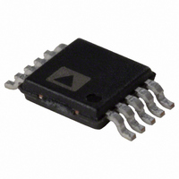
AD5161BRMZ50 Analog Devices Inc, AD5161BRMZ50 Datasheet - Page 14

AD5161BRMZ50
Manufacturer Part Number
AD5161BRMZ50
Description
IC POT DGTL 50K 256POS 10-MSOP
Manufacturer
Analog Devices Inc
Datasheet
1.AD5161BRMZ10.pdf
(20 pages)
Specifications of AD5161BRMZ50
Temperature Coefficient
45 ppm/°C Typical
Taps
256
Resistance (ohms)
50K
Number Of Circuits
1
Memory Type
Volatile
Interface
I²C, SPI
Voltage - Supply
2.7 V ~ 5.5 V
Operating Temperature
-40°C ~ 125°C
Mounting Type
Surface Mount
Package / Case
10-MSOP, Micro10™, 10-uMAX, 10-uSOP
Resistance In Ohms
50K
End To End Resistance
50kohm
No. Of Steps
256
Resistance Tolerance
± 30%
Supply Voltage Range
2.7V To 5.5V
Control Interface
Serial, I2C
No. Of Pots
Single
Number Of Elements
1
# Of Taps
256
Resistance (max)
50KOhm
Power Supply Requirement
Single
Single Supply Voltage (typ)
3/5V
Dual Supply Voltage (typ)
Not RequiredV
Single Supply Voltage (min)
2.7V
Single Supply Voltage (max)
5.5V
Dual Supply Voltage (min)
Not RequiredV
Dual Supply Voltage (max)
Not RequiredV
Operating Temp Range
-40C to 125C
Operating Temperature Classification
Automotive
Mounting
Surface Mount
Pin Count
10
Lead Free Status / RoHS Status
Lead free / RoHS Compliant
Lead Free Status / RoHS Status
Lead free / RoHS Compliant, Lead free / RoHS Compliant
Available stocks
Company
Part Number
Manufacturer
Quantity
Price
Part Number:
AD5161BRMZ50
Manufacturer:
ADI/亚德诺
Quantity:
20 000
Company:
Part Number:
AD5161BRMZ50-RL7
Manufacturer:
AD
Quantity:
1 140
AD5161
I
Table 7. Write Mode
Table 8. Read Mode
S = Start Condition
P = Stop Condition
A = Acknowledge
X = Don’t Care
W = Write
START BY
S 0 1 0 1 1 0
MASTER
2
C INTERFACE
S
SCL
SDA
SDA
SCL
0
Slave Address Byte
P
1
0
1
t
SLAVE ADDRESS BYTE
1
START BY
MASTER
1
S
0
FRAME 1
0
Slave Address Byte
SCL
SDA
t
AD0
2
1
1
1
1
0
W
t
3
Figure 41. Reading Data from a Previously Selected RDAC Register in Write Mode
0
1
1
A X
AD0
SLAVE ADDRESS BYTE
t
8
0
t
8
0
R/W
FRAME 1
1
RS
ACK BY
AD5161
t
9
Figure 39. I
AD0
9
1
Instruction Byte
Figure 40. Writing to the RDAC Register
SD
t
6
1
X
0
2
R
RS
C Interface Detailed Timing Diagram
X X X X X A
AD0
t
t
4
Rev. A | Page 14 of 20
9
SD
INSTRUCTION BYTE
R/W
A
ACK BY
AD5161
FRAME 2
X
9
D7
X
t
D7
1
7
R = Read
RS = Reset wiper to Midscale 80
SD = Shutdown connects wiper to B terminal and open circuits
A terminal. It does not change contents of wiper register.
D7, D6, D5, D4, D3, D2, D1, D0 = Data Bits.
X
D6
D6
X
D5
D7
RDAC REGISTER
X
D5
S
D4
FRAME 2
ACK BY
AD5161
t
D6
5
9
D3
D4
Data Byte
D7
1
D5
D2
t
2
D6
D3
D1
Data Byte
D4
D5
D0
DATA BYTE
NO ACK
BY MASTER
D2
H
D4
FRAME 3
D3
9
D3
STOP BY
MASTER
D1
D2
D2
D1
D0
D1
D0
P
ACK BY
AD5161
D0
A
t
10
9
STOP BY
MASTER
A P
P


