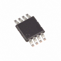
MAX5428EUA+ Maxim Integrated Products, MAX5428EUA+ Datasheet - Page 2

MAX5428EUA+
Manufacturer Part Number
MAX5428EUA+
Description
IC POT DGTL 1TIME PROGR 8-UMAX
Manufacturer
Maxim Integrated Products
Datasheet
1.MAX5428EUA.pdf
(10 pages)
Specifications of MAX5428EUA+
Taps
32
Resistance (ohms)
50K
Number Of Circuits
1
Temperature Coefficient
35 ppm/°C Typical
Memory Type
Non-Volatile
Interface
I²C, 2-Wire Serial
Voltage - Supply
2.7 V ~ 5.5 V
Operating Temperature
-40°C ~ 85°C
Mounting Type
Surface Mount
Package / Case
8-MSOP, Micro8™, 8-uMAX, 8-uSOP,
Resistance In Ohms
50K
Number Of Pots
Single
Taps Per Pot
32
Resistance
50 KOhms
Wiper Memory
Non Volatile
Digital Interface
Serial (2-Wire)
Operating Supply Voltage
5 V
Supply Current
1.5 uA
Maximum Operating Temperature
+ 85 C
Minimum Operating Temperature
- 40 C
Mounting Style
SMD/SMT
Supply Voltage (max)
5.5 V
Supply Voltage (min)
2.7 V
Lead Free Status / RoHS Status
Lead free / RoHS Compliant
ABSOLUTE MAXIMUM RATINGS
V
V
All Other Pins to GND.................................-0.3V to (V
Input and Output Latchup Immunity...............................±200mA
Maximum Continuous Current into H, L, and W
One-Time Programmable, Linear-Taper
Digital Potentiometers
Stresses beyond those listed under “Absolute Maximum Ratings” may cause permanent damage to the device. These are stress ratings only, and functional
operation of the device at these or any other conditions beyond those indicated in the operational sections of the specifications is not implied. Exposure to
absolute maximum rating conditions for extended periods may affect device reliability.
ELECTRICAL CHARACTERISTICS
(V
5.0V, T
2
DD
PP
DC PERFORMANCE
Resolution
End-to-End Resistance
End-to-End Resistance Tempco
Ratiometric Resistance Tempco
Integral Nonlinearity
Differential Nonlinearity
Full-Scale Error
Zero-Scale Error
Wiper Resistance
DIGITAL INPUTS (CS, U/D)
Input High Voltage
Input Low Voltage
Input Current
Input Capacitance
TIMING CHARACTERISTICS (Note 2)
U/D Mode to CS Setup
CS Hold to U/D Mode
U/D Step Hold to CS
U/D Step Low Time
DD
to GND..........................................................-0.3V to +12.0V
_______________________________________________________________________________________
to GND ...........................................................-0.3V to +6.0V
MAX5427 .................................................................±1.5mA
MAX5428 .................................................................±1.5mA
MAX5429 .................................................................±2.0mA
= 2.7V to 5.5V, V
A
= +25°C, unless otherwise noted.) (Note 1)
PARAMETER
PP
= GND, V
H
SYMBOL
= V
DNL
TC
INL
V
C
t
R
V
I
t
t
CU
t
IN
CI
IC
IL
IH
W
IL
IN
DD
R
, V
L
MAX5427
MAX5428
MAX5429
MAX5427/MAX5428
MAX5429
Potentiometer configuration, no load,
Figure 1
Potentiometer configuration, no load,
Figure 1
Potentiometer configuration, no load,
Figure 1
Potentiometer configuration, no load,
Figure 1
MAX5427 I
MAX5429 I
Figures 2, 3
Figures 2, 3
Figures 2, 3
Figures 2, 3
= GND, T
DD
+ 0.3V)
A
W
W
= -40°C to +85°C, unless otherwise noted. Typical values are at V
= 20µA; MAX5428 I
= 200µA
CONDITIONS
Continuous Power Dissipation (T
Operating Temperature Range ...........................-40°C to +85°C
Junction Temperature ......................................................+150°C
Storage Temperature Range .............................-65°C to +150°C
Lead Temperature (soldering, 10s) .................................+300°C
8-Pin µMAX (derate 4.5mW/°C above +70°C) .............362mW
8-Pin QFN-EP (derate 24.4mW/°C above +70°C)......1951mW
W
= 40µA;
37.5
0.7
MIN
V
100
7.5
32
75
50
50
DD
0
A
x
= +70°C)
±0.1
TYP
100
100
50
10
35
10
5
5
MAX
0.3
62.5
12.5
+0.5
V
125
-0.5
240
±1
±1
±1
DD
x
ppm/°C
ppm/°C
UNITS
Taps
LSB
LSB
LSB
LSB
k
µA
pF
ns
ns
ns
ns
V
V
DD
=


