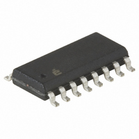
X9421YS16IZ-2.7 Intersil, X9421YS16IZ-2.7 Datasheet - Page 12

X9421YS16IZ-2.7
Manufacturer Part Number
X9421YS16IZ-2.7
Description
IC XDCP SGL 64-TAP 2.5K 16-SOIC
Manufacturer
Intersil
Series
XDCP™r
Datasheet
1.X9421WS16ZT1.pdf
(20 pages)
Specifications of X9421YS16IZ-2.7
Taps
64
Resistance (ohms)
2.5K
Number Of Circuits
1
Temperature Coefficient
300 ppm/°C Typical
Memory Type
Non-Volatile
Interface
SPI, 3-Wire Serial
Voltage - Supply
2.7 V ~ 5.5 V
Operating Temperature
-40°C ~ 85°C
Mounting Type
Surface Mount
Package / Case
16-SOIC (0.300", 7.5mm Width)
Resistance In Ohms
2.5K
Lead Free Status / RoHS Status
Lead free / RoHS Compliant
DC Electrical Specifications
ENDURANCE AND DATA RETENTION
CAPACITANCE
POWER-UP TIMING
NOTES:
Power-up Requirements
(Power-up sequencing can affect correct recall of the wiper
registers) The preferred power-on sequence is as follows:
First V
Voltage should not be applied to the potentiometer pins
before V
should be met, and any glitches or slope changes in the V
line should be held to <100mV if possible. Also, V
not reverse polarity by more than 0.5V. Recall of wiper
Minimum Endurance
Data Retention
1. Absolute Linearity is utilized to determine actual wiper voltage versus expected voltage as determined by wiper position when used as a
2. Relative Linearity is utilized to determine the actual change in voltage between two successive tap positions when used as a
3. MI = RTOT/63 or (V
4. Typical = Individual array resolution.
5. Parameters with MIN and/or MAX limits are 100% tested at +25°C, unless otherwise specified. Temperature limits established by characterization
6. Limits should be considered typical and are not production tested.
7. This parameter is not production tested. Parameter established by characterization.
t
SYMBOL
C
R
C
V
OUT
SYMBOL
potentiometer.
potentiometer. It is a measure of the error in step size.
and are not production tested.
I
I
V
SYMBOL
V
IN
CC
CC1
CC2
I
I
V
I
SB
LO
OL
LI
IH
IL
CC
(Note 5)
(Note 5)
(Note 5)
CC
and then the potentiometer pins, R
is applied. The V
V
(Active)
V
(Nonvolatile Write)
V
Input Leakage Current
Output Leakage Current
Input HIGH Voltage
Input LOW Voltage
Output LOW Voltage
CC
CC
CC
PARAMETER
V
Supply Current
Supply Current
Current (Standby)
Output Capacitance (SO)
Input Capacitance (A0, SI, and SCK)
CC
PARAMETER
H
Power-up Ramp
- V
L
)/63, single pot
12
CC
ramp rate specification
(Over the recommended operating conditions unless otherwise specified).
PARAMETER
f
Other Inputs = V
f
Other Inputs = V
SCK = SI = V
V
V
I
TEST
SCK
SCK
OL
IN
OUT
= 3mA
= V
H
= 2MHz, SO = Open,
= 2MHz, SO = Open,
, R
= V
SS
L
CC
SS
TEST CONDITIONS
, and R
to V
to V
SS
should
CC
, Addr. = V
SS
SS
CC
100,000
CC
W
MIN
100
.
X9421
SS
position will not be complete until V
value.
MIN
0.2
TYP
Data Changes per Bit per Register
Years
8
6
V
(Note 5)
CC
MIN
-0.5
x 0.7
MAX
UNITS
50
(Note 6)
pF
pF
TYP
UNITS
LIMITS
CC
V
V
(Note 5)
CC
CC
reaches its final
MAX
TEST CONDITIONS
400
3.5
0.4
10
10
3
+ 0.3
x 0.1
V
V/msec
UNITS
V
OUT
IN
= 0V
January 14, 2009
= 0V
UNITS
mA
µA
µA
µA
µA
FN8196.4
V
V
V


