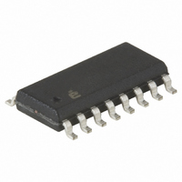
X9421YS16IZ-2.7T1 Intersil, X9421YS16IZ-2.7T1 Datasheet - Page 9

X9421YS16IZ-2.7T1
Manufacturer Part Number
X9421YS16IZ-2.7T1
Description
IC XDCP SGL 64-TAP 2.5K 16-SOIC
Manufacturer
Intersil
Series
XDCP™r
Datasheet
1.X9421WS16ZT1.pdf
(20 pages)
Specifications of X9421YS16IZ-2.7T1
Taps
64
Resistance (ohms)
2.5K
Number Of Circuits
1
Temperature Coefficient
300 ppm/°C Typical
Memory Type
Non-Volatile
Interface
SPI, 3-Wire Serial
Voltage - Supply
2.7 V ~ 5.5 V
Operating Temperature
-40°C ~ 85°C
Mounting Type
Surface Mount
Package / Case
16-SOIC (0.300", 7.5mm Width)
Resistance In Ohms
2.5K
Lead Free Status / RoHS Status
Lead free / RoHS Compliant
Read Wiper Counter Register
Write Wiper Counter Register
Read Data Register
Write Data Register
XFR Data Register to Wiper
Counter Register
XFR Wiper Counter Register to Data
Register
Increment/Decrement Wiper
Counter Register
Read Status (WIP bit)
Instruction Format
NOTES:
Read Wiper Counter Register (WCR)
Write Wiper Counter Register (WCR)
Read Data Register (DR)
Read the contents of the Register pointed to by R1 - R0.
Write Data Register (DR)
Write a new value to the Register pointed to by R1 - R0.
FALLING
FALLING
FALLING
FALLING
1. “A0”: stands for the device addresses sent by the master.
2. WPx refers to wiper position data in the Wiper Counter Register
3. “D”: stands for the decrement operation, SI held LOW during active SCK phase (high).
EDGE
EDGE
EDGE
EDGE
CS
CS
CS
“I”: stands for the increment operation, SI held HIGH during
active SCK phase (high).
CS
INSTRUCTION
0
0
0
IDENTIFIER
IDENTIFIER
0
IDENTIFIER
IDENTIFIER
DEVICE
DEVICE
DEVICE
DEVICE
TYPE
TYPE
TYPE
1
1
TYPE
1
1
0
0
0
0
1
1
1
1
ADDRESSES
1
1
1
1
ADDRESSES
ADDRESSES
ADDRESSES
DEVICE
DEVICE
DEVICE
DEVICE
1
1
1
1
9
I
1
1
1
1
1
1
0
0
3
0
0
0
0
A
0
A0
A0
A0
I
0
0
0
1
1
1
0
1
2
INSTRUCTION
1
INSTRUCTION
INSTRUCTION
1
1
1
OPCODE
INSTRUCTION
I
0
1
1
0
0
1
1
0
1
INSTRUCTION SET
OPCODE
1
OPCODE
OPCODE
0
0
0
0
I
1
0
1
0
1
0
0
1
0
1
1
TABLE 3. INSTRUCTION SET
0
0
1/0
1/0
1/0
1/0
R
0
1
0
0
0
0
1
1
ADDRESSES
R
1
REGISTER
R1
0
ADDRESSES
1/0
1/0
1/0
1/0
0
R
R
0
0
0
0
0
REGISTER
X9421
0
0
0
R0
0
0
0
0
0
0
0
0
0
0
0
0
0
0
0
0
0
0
0
0
0
0
0
0
0
1
0
0
0
0
Read the contents of the Wiper Counter Register
Write new value to the Wiper Counter Register
Read the contents of the Data Register pointed to by R
Write new value to the Data Register pointed to by R
Transfer the contents of the Data Register pointed to by R
R
Transfer the contents of the Wiper Counter
Register to the Data Register pointed to by R
Enable Increment/decrement of the Wiper Counter Register
Read the status of the internal write cycle, by checking the WIP
bit.
0
WP
(SENT BY HOST ON SI)
0
5
WP5
0
to the Wiper Counter Register
WP5
WP
WP5
DATA BYTE
4
(SENT BY HOST ON SI)
(SENT BY X9421 ON SO)
(SENT BY X9421 ON SO)
WP4
WP
WP4
WIPER POSITION
3
DATA BYTE
WP4 WP3
DATA BYTE
WP3
WP
2
WP3
WP
OPERATION
WP2
1
WP2
WP2
WP
0
WP1
WP1
WP1 WP0
RISING
EDGE
CS
WP0
WP0
1
January 14, 2009
- R
RISING
HIGH-VOLTAGE
EDGE
0
WRITE CYCLE
RISING
RISING
EDGE
EDGE
CS
CS
FN8196.4
CS
1
- R
1
- R
0
1
-
0


