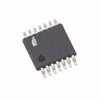
X9429YV14IZT1 Intersil, X9429YV14IZT1 Datasheet - Page 4

X9429YV14IZT1
Manufacturer Part Number
X9429YV14IZT1
Description
IC XDCP SGL 64-TAP 2.5K 14-TSSOP
Manufacturer
Intersil
Series
XDCP™r
Datasheet
1.X9429WS16ZT1.pdf
(20 pages)
Specifications of X9429YV14IZT1
Taps
64
Resistance (ohms)
2.5K
Number Of Circuits
1
Temperature Coefficient
300 ppm/°C Typical
Memory Type
Non-Volatile
Interface
I²C, 2-Wire Serial
Voltage - Supply
4.5 V ~ 5.5 V
Operating Temperature
-40°C ~ 85°C
Mounting Type
Surface Mount
Package / Case
14-TSSOP
Resistance In Ohms
2.5K
Lead Free Status / RoHS Status
Lead free / RoHS Compliant
Pinouts
Pin Assignments
Pin Descriptions
Host Interface Pins
SERIAL CLOCK (SCL)
The SCL input is used to clock data into and out of the
X9429.
SERIAL DATA (SDA)
SDA is a bidirectional pin used to transfer data into and out of
the device. It is an open drain output and may be wire-ORed
with any number of open drain or open collector outputs. An
open drain output requires the use of a pull-up resistor. For
selecting typical values, refer to the guidelines for calculating
typical values on the bus pull-up resistors graph.
DEVICE ADDRESS (A
The Address inputs are used to set the least significant 3 bits
of the 8-bit slave address. A match in the slave address
serial data stream must be made with the Address input in
order to initiate communication with the X9429. A maximum
of 8 devices may occupy the 2-wire serial bus.
TSSOP PIN
1, 2, 3
10
11
12
13
14
4
5
6
7
8
9
SDA
SCL
VSS
NC
NC
NC
A2
12, 3, 7, 15
SOIC PIN
(14 LD TSSOP)
0
1
2
3
4
5
6
7
10
11
12
13
14
16
, A
4
5
6
8
9
TOP VIEW
2
X9429
X9429
, A
4
3
)
14
13
12
11
10
9
8
SYMBOL
R
R
R
SDA
SCL
V
W
V
WP
NC
H
A2
A0
A3
L
SS
CC
/V
/V
/V
W
H
L
V
R
R
R
A3
A0
WP
CC
L
H
W
/V
/V
/V
L
H
W
No Connect
Device Address for 2-wire bus.
Serial Clock for 2-wire bus.
Serial Data Input/Output for 2-wire bus.
System Ground
Hardware Write Protect
Device Address for 2-wire bus.
Device Address for 2-wire bus.
Wiper Terminal of the Potentiometer.
High Terminal of the Potentiometer.
Low Terminal of the Potentiometer.
System Supply Voltage
X9429
Potentiometer Pins
R
The R
connections on either end of a mechanical potentiometer.
R
The wiper outputs are equivalent to the wiper output of a
mechanical potentiometer.
HARDWARE WRITE PROTECT INPUT WP
The WP pin when low prevents nonvolatile writes to the Data
Registers.
Principals of Operation
The X9429 is a highly integrated microcircuit incorporating a
resistor array and its associated registers and counters and
the serial interface logic providing direct communication
between the host and the XDCP potentiometers.
Serial Interface
The X9429 supports a bidirectional bus oriented protocol.
The protocol defines any device that sends data onto the
H
W
/V
/V
H
W
H
, R
/V
L
H
BRIEF DESCRIPTION
/V
and R
L
SDA
SCL
VSS
NC
NC
NC
NC
A2
L
/V
L
inputs are equivalent to the terminal
(16 LD SOIC)
1
2
3
4
5
6
7
8
TOP VIEW
X9429
X9429
16
15
14
13
12
11
10
9
V
NC
R
R
R
A3
A0
WP
CC
L
H
W
/V
/V
/V
L
H
W
October 13, 2008
FN8248.3


