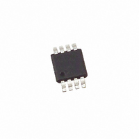
X9317WM8I-2.7 Intersil, X9317WM8I-2.7 Datasheet - Page 7

X9317WM8I-2.7
Manufacturer Part Number
X9317WM8I-2.7
Description
IC DIGITAL POT 10K 100TP 8MSOP
Manufacturer
Intersil
Series
XDCP™r
Datasheet
1.X9317WP.pdf
(15 pages)
Specifications of X9317WM8I-2.7
Taps
100
Resistance (ohms)
10K
Number Of Circuits
1
Temperature Coefficient
300 ppm/°C Typical
Memory Type
Non-Volatile
Interface
Up/Down (3-Wire)
Voltage - Supply
2.7 V ~ 5.5 V
Operating Temperature
-40°C ~ 85°C
Mounting Type
Surface Mount
Package / Case
8-MSOP, Micro8™, 8-uMAX, 8-uSOP,
Resistance In Ohms
10K
Number Of Elements
1
# Of Taps
100
Resistance (max)
10KOhm
Power Supply Requirement
Single
Interface Type
Serial (3-Wire)
Single Supply Voltage (typ)
3.3/5V
Dual Supply Voltage (typ)
Not RequiredV
Single Supply Voltage (min)
2.7V
Single Supply Voltage (max)
5.5V
Dual Supply Voltage (min)
Not RequiredV
Dual Supply Voltage (max)
Not RequiredV
Operating Temp Range
-40C to 85C
Operating Temperature Classification
Industrial
Mounting
Surface Mount
Pin Count
8
Package Type
MSOP
Lead Free Status / RoHS Status
Contains lead / RoHS non-compliant
Endurance and Data Retention
NOTES:
Test Circuit
AC Electrical Specifications
1. Absolute linearity is utilized to determine actual wiper voltage versus expected voltage = [V(R
2. Relative linearity is a measure of the error in step size between taps = [V(R
3. 1 Ml = Minimum Increment = [V(R
4. Typical values are for T
5. This parameter is not 100% tested.
6. Ratiometric temperature coefficient = (V(R
7. Measured with wiper at tap position 99, R
8. Parameters with MIN and/or MAX limits are 100% tested at +25°C, unless otherwise specified. Temperature limits established by characterization
V(R
to 99.
and are not production tested.
t
t
t
PU
lD
DI
SYMBOL
(Note 5)
(Note 5)
(Note 5)
t
W(n)(expected)
t
t
CPHNS
R
(Note 5)
(Note 5)
CPHS
t
t
R
(Note 5)
t
R
CYC
t
WR
t
t
t
t
IW
V
Cl
lH
lC
lL
, t
W
CC
F
TEST POINT
FORCE
CURRENT
Minimum Endurance
) = n(V(R
Data Retention
PARAMETER
CS to INC Setup
INC HIGH to U/D Change
U/D to INC Setup
INC LOW Period
INC HIGH Period
INC Inactive to CS Inactive
CS Deselect Time (STORE)
CS Deselect Time (NO STORE)
INC to R
INC Cycle Time
INC Input Rise and Fall Time
Power-up to Wiper Stable
V CC Power-up Rate
Store Cycle
Equivalent Circuit
A
R
= +25°C and nominal supply voltage.
H
H
W
)-V(R
7
Change
10pF
H
L
))/99 + V(R
)-V(R
V
C
V
CC
H
CC
L
R
L
)]/99.
= 5V ±10%, T
W
TOTAL
= 5V ±10%, T
grounded, using test circuit.
PARAMETER
)
R
T1(n)
W
L
), with n from 0 to 99.
25pF
C
-V(R
W
W
A
)
A
10pF
T2(n)
= Full Operating Temperature Range, unless otherwise stated.
= Full Operating Temperature Range.
C
L
)/[V(R
R
X9317
L
100,000
W
MIN
100
)
T1(n)
AC Conditions of Test
W(n+1)
Input pulse levels
Input rise and fall times
Input reference levels
(T1-T2) x 10
)-(V(R
(Note 8)
6
W(n)
MIN
100
960
960
100
0.2
], with T1 and T2 being 2 temperatures, and n from 0
50
10
1
1
2
) - MI)]/MI.
W(n)(actual)
(Note 4)
Data changes per bit
)-V(R
TYP
1
5
W(n)(expected)
0V to 3V
10ns
1.5V
Years
UNIT
(Note 8)
MAX
500
50
10
5
5
)]/MI
December 16, 2009
UNIT
V/ms
FN8183.6
ms
ms
ns
ns
µs
ns
ns
µs
ns
µs
µs
µs
µs


