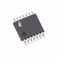
X9421WV14IZ-2.7 Intersil, X9421WV14IZ-2.7 Datasheet - Page 4

X9421WV14IZ-2.7
Manufacturer Part Number
X9421WV14IZ-2.7
Description
IC XDCP SGL 64-TAP 10K 14-TSSOP
Manufacturer
Intersil
Series
XDCP™r
Datasheet
1.X9421WS16ZT1.pdf
(20 pages)
Specifications of X9421WV14IZ-2.7
Taps
64
Resistance (ohms)
10K
Number Of Circuits
1
Temperature Coefficient
300 ppm/°C Typical
Memory Type
Non-Volatile
Interface
SPI, 3-Wire Serial
Voltage - Supply
2.7 V ~ 5.5 V
Operating Temperature
-40°C ~ 85°C
Mounting Type
Surface Mount
Package / Case
14-TSSOP
Resistance In Ohms
10K
Lead Free Status / RoHS Status
Lead free / RoHS Compliant
Pin Assignments
Pin Descriptions
Host Interface Pins
SERIAL OUTPUT (SO)
SO is a push/pull serial data output pin. During a read cycle,
data is shifted out on this pin. Data is clocked out by the
falling edge of the serial clock.
SERIAL INPUT
SI is the serial data input pin. All opcodes, byte addresses
and data to be written to the potentiometer and pot register
are input on this pin. Data is latched by the rising edge of the
serial clock.
SERIAL CLOCK (SCK)
The SCK input is used to clock data into and out of the
X9421.
PIN NO.
TSSOP
2, 3
10
12
13
14
11
1
4
5
6
7
8
9
SCK
VSS
NC
NC
CS
S0
SI
1
2
3
4
5
6
7
3, 1, 7, 5
(14 LD TSSOP)
PIN NO.
SOIC
TOP VIEW
10
12
13
14
16
2
4
5
6
8
9
X9421
4
14
13
12
10
11
9
8
VCC
R
R
R
HOLD
A0
WP
SYMBOL
L
H
W
R
R
HOLD
R
/V
/V
VCC
SCK
VSS
/V
W
WP
H
SO
NC
CS
A0
L
SI
L
H
W
/V
/V
/V
W
H
L
Serial Data Output
No Connect
Chip Select
Serial Clock
Serial Data Input
System Ground
Hardware Write Protect
Device Address
Device select. Pause the serial bus.
Wiper Terminal of the Potentiometer.
High Terminal of the Potentiometer.
Low Terminal of the Potentiometer.
System Supply Voltage
X9421
CHIP SELECT (CS)
When CS is HIGH, the X9421 is deselected and the SO pin
is at high impedance, and (unless an internal write cycle is
underway) the device will be in the standby state. CS LOW
enables the X9421, placing it in the active power mode. It
should be noted that after a power-up, a HIGH to LOW
transition on CS is required prior to the start of any
operation.
HOLD (HOLD)
HOLD is used in conjunction with the CS pin to select the
device. Once the part is selected and a serial sequence is
underway, HOLD may be used to pause the serial
communication with the controller without resetting the serial
sequence. To pause, HOLD must be brought LOW while
SCK is LOW. To resume communication, HOLD is brought
HIGH, again while SCK is LOW. If the pause feature is not
used, HOLD should be held HIGH at all times.
DESCRIPTION
SCK
VSS
NC
SO
NC
CS
NC
SI
1
2
3
4
5
6
7
8
(16 LD SOIC)
TOP VIEW
X9421
16
15
14
13
12
11
10
9
VCC
NC
R
R
R
ISEN
AO
WP
L
H
W
/V
/V
/V
L
H
W
January 14, 2009
FN8196.4


