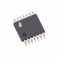
X9429YV14IZ-2.7 Intersil, X9429YV14IZ-2.7 Datasheet

X9429YV14IZ-2.7
Specifications of X9429YV14IZ-2.7
Related parts for X9429YV14IZ-2.7
X9429YV14IZ-2.7 Summary of contents
Page 1
... SS CAUTION: These devices are sensitive to electrostatic discharge; follow proper IC Handling Procedures. 1-888-INTERSIL or 1-888-468-3774 XDCP is a trademark of Intersil Americas Inc. Copyright Intersil Americas Inc. 2005, 2008. All Rights Reserved All other trademarks mentioned are the property of their respective owners. X9429 Low Noise/Low Power/2-Wire Bus FN8248 ...
Page 2
... X9429 YVZF X9429YV14I-2.7* X9429 YVG X9429YV14IZ-2.7* (Note) X9429 YVZG *Add "T1" suffix for tape and reel. **Add "T1" suffix for tape and reel.Please refer to TB347 for details on reel specifications. NOTE: These Intersil Pb-free plastic packaged products employ special Pb-free material sets, molding compounds/die attach materials, and 100% matte tin plate plus anneal (e3 termination finish, which is RoHS compliant and compatible with both SnPb and Pb-free soldering operations) ...
Page 3
Detailed Functional Diagram V CC SCL INTERFACE SDA AND A3 CONTROL CIRCUITRY Circuit Level Applications • Vary the Gain of a Voltage Amplifier • Provide Programmable DC Reference Voltages for Comparators and Detectors • Control ...
Page 4
Pinouts X9429 (14 LD TSSOP) TOP VIEW X9429 10 SCL SDA 8 7 VSS Pin Assignments TSSOP PIN SOIC PIN 12, 3, ...
Page 5
The device controlling the transfer is a master and the device being controlled is the slave. The master will always initiate data transfers and provide the clock for both ...
Page 6
Four of the seven instructions end with the transmission of the instruction byte. The basic sequence is illustrated in Figure 3. These two-byte instructions exchange data between the Wiper Counter Register and one of the Data Registers. A transfer from ...
Page 7
INSTRUCTION Read Wiper Counter Register 1 0 Write Wiper Counter Register 1 0 Read Data Register 1 0 Write Data Register 1 1 XFR Data Register to Wiper 1 1 Counter Register XFR Wiper Counter 1 ...
Page 8
INC/DEC CMD ISSUED SCL SDA FIGURE 6. INCREMENT/DECREMENT TIMING LIMITS SCL FROM MASTER DATA OUTPUT FROM TRANSMITTER DATA OUTPUT FROM RECEIVER START FIGURE 7. ACKNOWLEDGE RESPONSE FROM RECEIVER 8 X9429 VOLTAGE OUT 1 T WRID 8 ...
Page 9
SERIAL DATA PATH FROM INTERFACE CIRCUITRY REGISTER 0 REGISTER 2 IF WCR = 00[H] THEN WCR = 3F[H] THEN FIGURE 8. ...
Page 10
ONE 6-BIT WIPER COUNTER REGISTER FOR EACH XDCP. {D5~D0}: These bits specify the wiper position of the respective XDCP. The Wiper Counter Register is loaded on Instruction Format NOTES: 1. “MACK”/”SACK”: stands for the acknowledge sent by the master/slave. 2. ...
Page 11
XFR Data Register (DR) to Wiper Counter Register (WCR) DEVICE S TYPE DEVICE INSTRUCTION T S IDENTIFIER ADDRESSES XFR Wiper Counter Register ...
Page 12
... Thermal Resistance (Typical, Note 1) 14 Lead TSSOP . . . . . . . . . . . . . . . . . . . . . . . . . . . . 16 Lead SOIC . . . . . . . . . . . . . . . . . . . . . . . . . . . . . Temperature Under Bias . . . . . . . . . . . . . . . . . . . . .-65°C to +135°C Storage Temperature . . . . . . . . . . . . . . . . . . . . . . . .-65°C to +150°C Pb-Free Reflow Profile .see link below http://www.intersil.com/pbfree/Pb-FreeReflow.asp Operating Conditions Temperature Range Commercial . . . . . . . . . . . . . . . . . . . . . . . . . . . . . . . 0°C to +70°C Industrial .-40°C to +85°C TEST CONDITIONS +25° ...
Page 13
SYMBOL PARAMETER I Output Leakage Current LO V Input HIGH Voltage IH V Input LOW Voltage IL V Output LOW voltage OL ENDURANCE AND DATA RETENTION PARAMETER Minimum Endurance Data Retention CAPACITANCE SYMBOL C (Note 5) Input/output capacitance (SDA) I/O ...
Page 14
AC TIMING (Over recommended operating conditions) SYMBOL f Clock Frequency SCL t Clock Cycle Time CYC t Clock High Time HIGH t Clock Low Time LOW t Start Setup Time SU:STA t Start Hold Time HD:STA t Stop Setup Time ...
Page 15
Timing Diagrams Start and Stop Timing (START) SCL t SU:STA SDA Input Timing t CYC SCL SDA t SU:DAT Output Timing SCL SDA XDCP Timing (for All Load Instructions) SCL SDA X9429 ...
Page 16
XDCP Timing (for Increment/Decrement Instruction) SCL SDA WIPER REGISTER ADDRESS Write Protect and Device Address Pins Timing SCL SDA WP A0, A2, A3 Applications information Basic Configurations of Electronic Potentiometers V R THREE TERMINAL POTENTIOMETER; VARIABLE ...
Page 17
Application Circuits NONINVERTING AMPLIFIER – (1 OFFSET VOLTAGE ADJUSTMENT – 100kΩ + TL072 10kΩ 10kΩ 10kΩ +5V 17 X9429 ...
Page 18
Application Circuits (continued) ATTENUATOR – All -1/2 ≤ G ≤ +1/2 INVERTING AMPLIFIER – ...
Page 19
Thin Shrink Small Outline Plastic Packages (TSSOP) N INDEX 0.25(0.010) E AREA E1 - 0.05(0.002) SEATING PLANE - -C- α 0.10(0.004) 0.10(0.004 NOTES: 1. These package ...
Page 20
... Accordingly, the reader is cautioned to verify that data sheets are current before placing orders. Information furnished by Intersil is believed to be accurate and reliable. However, no responsibility is assumed by Intersil or its subsidiaries for its use; nor for any infringements of patents or other rights of third parties which may result from its use ...


