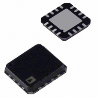
ADN2850BCP250 Analog Devices Inc, ADN2850BCP250 Datasheet - Page 15

ADN2850BCP250
Manufacturer Part Number
ADN2850BCP250
Description
IC DGTL RHEO DL 1024POS 16LFCSP
Manufacturer
Analog Devices Inc
Specifications of ADN2850BCP250
Taps
1024
Resistance (ohms)
250K
Number Of Circuits
2
Temperature Coefficient
35 ppm/°C Typical
Memory Type
Non-Volatile
Interface
4-Wire SPI Serial
Voltage - Supply
3 V ~ 5.5 V, ±2.25 V ~ 2.75 V
Operating Temperature
-40°C ~ 85°C
Mounting Type
Surface Mount
Package / Case
16-LFCSP
Resistance In Ohms
250K
Number Of Elements
2
# Of Taps
1024
Resistance (max)
250KOhm
Power Supply Requirement
Single/Dual
Interface Type
Serial (4-Wire/SPI)
Single Supply Voltage (typ)
5V
Dual Supply Voltage (typ)
±2.5V
Single Supply Voltage (min)
3V
Single Supply Voltage (max)
5.5V
Dual Supply Voltage (min)
±2.25V
Dual Supply Voltage (max)
±2.75V
Operating Temp Range
-40C to 85C
Operating Temperature Classification
Industrial
Mounting
Surface Mount
Pin Count
16
Lead Free Status / RoHS Status
Contains lead / RoHS non-compliant
For Use With
EVAL-ADN2850-25EBZ - BOARD EVALUATION FOR ADN2850-25
Lead Free Status / RoHS Status
Not Compliant, Contains lead / RoHS non-compliant
resistor and the capacitive loading at the SDO-to-SDI interface may
require additional time delay between subsequent devices.
When two ADN2850s are daisy-chained, 48 bits of data are
required. The first 24 bits (formatted 4-bit command, 4-bit
address, and 16-bit data) go to U2, and the second 24 bits with
the same format go to U1. Keep CS low until all 48 bits are
clocked into their respective serial registers. CS is then pulled
high to complete the operation.
TERMINAL VOLTAGE OPERATING RANGE
The positive V
define the boundary conditions for proper 2-terminal digital
resistor operation. Supply signals present on Terminal B, and
Terminal W that exceed V
forward-biased diodes (see Figure 29).
The GND pin of the ADN2850 is primarily used as a digital
ground reference. To minimize the digital ground bounce,
the ADN2850 ground terminal should be joined remotely to
the common ground (see Figure 30). The digital input control
signals to the ADN2850 must be referenced to the device
ground pin (GND) and must satisfy the logic level defined in
the Specifications section. An internal level-shift circuit ensures
that the common-mode voltage range of the three terminals
CONTROLLER
MICRO-
SCLK SS
Figure 29. Maximum Terminal Voltages Set by V
MOSI
Figure 28. Daisy-Chain Configuration Using SDO
DD
and negative V
SDI
ADN2850
CS
U1
DD
CLK
or V
SDO
SS
SS
power supplies of the ADN2850
are clamped by the internal
V
DD
R
2.2kΩ
P
SDI
CS
V
ADN2850
V
W
B
SS
DD
DD
U2
and V
CLK
SDO
SS
Rev. C | Page 15 of 28
extends from V
Power-Up Sequence
Because there are diodes to limit the voltage compliance at
Terminal B, and Terminal W (see Figure 29), it is important to
power V
B, and Terminal W. Otherwise, the diode is forward-biased such
that V
applying 5 V across Terminal W and Terminal B prior to V
causes the V
the device, but it might affect the rest of the user’s system. The
ideal power-up sequence is GND, V
and V
inputs is not important as long as they are powered after V
and V
Regardless of the power-up sequence and the ramp rates of the
power supplies, when V
preset activates, which restores the EEMEM values to the RDAC
registers.
Layout and Power Supply Bypassing
It is a good practice to employ compact, minimum lead-length
layout design. The leads to the input should be as direct as
possible with a minimum conductor length. Ground paths
should have low resistance and low inductance.
Similarly, it is good practice to bypass the power supplies with
quality capacitors for optimum stability. Bypass supply leads to
the device with 0.01 μF to 0.1 μF disk or chip ceramic capacitors.
Also, apply low ESR, 1 μF to 10 μF tantalum or electrolytic
capacitors at the supplies to minimize any transient disturbance
(see Figure 30).
DD
B
SS
, and V
.
V
V
DD
and V
DD
SS
and V
DD
10µF
10µF
W
SS
C3
C4
terminal to exhibit 4.3 V. It is not destructive to
SS
. The order of powering V
are powered unintentionally. For example,
SS
to V
Figure 30. Power Supply Bypassing
+
+
first before applying any voltage to Terminal
0.1µF
0.1µF
DD
C1
C2
DD
, regardless of the digital input level.
and V
SS
are powered, the power-on
DD
V
V
DD
SS
and V
ADN2850
GND
B
, V
SS
W
, digital inputs,
, and the digital
ADN2850
DD
DD


