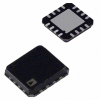
ADN2850BCP250 Analog Devices Inc, ADN2850BCP250 Datasheet - Page 21

ADN2850BCP250
Manufacturer Part Number
ADN2850BCP250
Description
IC DGTL RHEO DL 1024POS 16LFCSP
Manufacturer
Analog Devices Inc
Specifications of ADN2850BCP250
Taps
1024
Resistance (ohms)
250K
Number Of Circuits
2
Temperature Coefficient
35 ppm/°C Typical
Memory Type
Non-Volatile
Interface
4-Wire SPI Serial
Voltage - Supply
3 V ~ 5.5 V, ±2.25 V ~ 2.75 V
Operating Temperature
-40°C ~ 85°C
Mounting Type
Surface Mount
Package / Case
16-LFCSP
Resistance In Ohms
250K
Number Of Elements
2
# Of Taps
1024
Resistance (max)
250KOhm
Power Supply Requirement
Single/Dual
Interface Type
Serial (4-Wire/SPI)
Single Supply Voltage (typ)
5V
Dual Supply Voltage (typ)
±2.5V
Single Supply Voltage (min)
3V
Single Supply Voltage (max)
5.5V
Dual Supply Voltage (min)
±2.25V
Dual Supply Voltage (max)
±2.75V
Operating Temp Range
-40C to 85C
Operating Temperature Classification
Industrial
Mounting
Surface Mount
Pin Count
16
Lead Free Status / RoHS Status
Contains lead / RoHS non-compliant
For Use With
EVAL-ADN2850-25EBZ - BOARD EVALUATION FOR ADN2850-25
Lead Free Status / RoHS Status
Not Compliant, Contains lead / RoHS non-compliant
APPLICATIONS INFORMATION
GAIN CONTROL COMPENSATION
A digital resistor is commonly used in gain control such as the
noninverting gain amplifier shown in Figure 34.
When the RDAC B terminal parasitic capacitance is connected
to the op amp noninverting node, it introduces a zero for the 1/β
term with 20 dB/dec, whereas a typical op amp gain bandwidth
product (GBP) has −20 dB/dec characteristics. A large R2 and
finite C1 can cause the frequency of this zero to fall well below
the crossover frequency. Therefore, the rate of closure becomes
40 dB/dec, and the system has a 0° phase margin at the crossover
frequency. If an input is a rectangular pulse or step function, the
output can ring or oscillate. Similarly, it is also likely to ring when
switching between two gain values; this is equivalent to a stop
change at the input.
Depending on the op amp GBP, reducing the feedback resistor
might extend the frequency of the zero far enough to overcome
the problem. A better approach is to include a compensation
capacitor, C2, to cancel the effect caused by C1. Optimum
compensation occurs when R1 × C1 = R2 × C2. This is not
an option because of the variation of R2. As a result, one can
use the previous relationship and scale C2 as if R2 were at its
maximum value. Doing this might overcompensate and
compromise the performance when R2 is set at low values.
Alternatively, it avoids the ringing or oscillation at the worst
case. For critical applications, find C2 empirically to suit the
oscillation. In general, C2 in the range of a few picofarads to no
more than a few tenths of picofarads is usually adequate for the
compensation.
Similarly, W and A terminal capacitances are connected to the
output (not shown); their effect at this node is less significant
and the compensation can be avoided in most cases.
PROGRAMMABLE LOW-PASS FILTER
In analog-to-digital conversions (ADCs), it is common to
include an antialiasing filter to band limit the sampling signal.
Therefore, the dual-channel ADN2850 can be used to construct
a second-order Sallen-Key low-pass filter, as shown in Figure 35.
Figure 34. Typical Noninverting Gain Amplifier
47kΩ
R1
11pF
C1
V
I
2.2pF
U1
C2
250kΩ
B
W
R2
V
O
Rev. C | Page 21 of 28
O
The design equations are
First, users should select convenient values for the capacitors.
To achieve maximally flat bandwidth, where Q = 0.707, let C1
be twice the size of C2 and let R1 equal R2. As a result, the user
can adjust R1 and R2 concurrently to the same setting to
achieve the desirable bandwidth.
PROGRAMMABLE OSCILLATOR
In a classic Wien bridge oscillator, the Wien network (R||C, R'C')
provides positive feedback, whereas R1 and R2 provide negative
feedback (see Figure 36).
V
I
Q =
CONCURRENTLY
V
ω
V
R
2.2nF
O
O
R = R' = ADN2850
R2B = AD5231
D1 = D2 = 1N4148
I
Figure 36. Programmable Oscillator with Amplitude Control
R1
ADJUSTED
=
=
W
R1
C
B
S
1
ADJUSTMENT
2
FREQUENCY
R1
C1
+
25kΩ
R2
ω
+
Q
Figure 35. Sallen-Key Low-Pass Filter
ω
R
f
1
R2
R2
C1
f
R
S
B
2
W
1
C2
+
B
C2
C2
ω
W
f
2
VP
B
R1
1kΩ AMPLITUDE
C1
10kΩ
2.2nF
W
R2B
+
–
OP1177
–2.5V
C'
+2.5V
V+
V–
ADJUSTMENT
A
AD8601
+2.5V
–2.5V
25kΩ
W
U1
A
R'
2.1kΩ
V+
V–
R2A
B
U1
D2
D1
ADN2850
V
O
V
O
(10)
(11)
(12)


