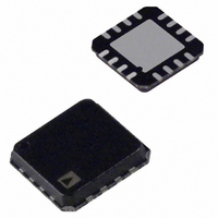
ADN2850BCP250-RL7 Analog Devices Inc, ADN2850BCP250-RL7 Datasheet - Page 22

ADN2850BCP250-RL7
Manufacturer Part Number
ADN2850BCP250-RL7
Description
IC DGTL RHEO DL 25K 9BIT16LFCSP
Manufacturer
Analog Devices Inc
Datasheet
1.ADN2850BCPZ250-RL7.pdf
(28 pages)
Specifications of ADN2850BCP250-RL7
Rohs Status
RoHS non-compliant
Taps
1024
Resistance (ohms)
250K
Number Of Circuits
2
Temperature Coefficient
35 ppm/°C Typical
Memory Type
Non-Volatile
Interface
4-Wire SPI Serial
Voltage - Supply
3 V ~ 5.5 V, ±2.25 V ~ 2.75 V
Operating Temperature
-40°C ~ 85°C
Mounting Type
Surface Mount
Package / Case
16-LFCSP
Resistance In Ohms
250K
For Use With
EVAL-ADN2850-25EBZ - BOARD EVALUATION FOR ADN2850-25
ADN2850
At the resonant frequency, f
the positive feedback causes the circuit to oscillate. With R = R
C = C
where R is equal to R
At resonance, setting R2/R1 = 2 balances the bridge. In practice,
R2/R1 should be set slightly larger than 2 to ensure that the
oscillation can start. On the other hand, the alternate turn-on
of the diodes, D1 and D2, ensures that R2/R1 is smaller than 2,
momentarily stabilizing the oscillation.
When the frequency is set, the oscillation amplitude can be
turned by R2B because
V
selection of R2B, an equilibrium is reached such that V
converges. R2B can be in series with a discrete resistor to
increase the amplitude, but the total resistance cannot be too
large to saturate the output.
In Figure 35 and Figure 36, the frequency tuning requires that
both RDACs be adjusted concurrently to the same settings.
Because the two channels might be adjusted one at a time, an
intermediate state occurs that might not be acceptable for some
applications. Of course, the increment/decrement instructions
(Instruction 5, Instruction 7, Instruction 13, and Instruction 15)
can all be used. Different devices can also be used in daisy-chain
mode so that parts can be programmed to the same settings
simultaneously.
OPTICAL TRANSMITTER CALIBRATION WITH
ADN2841
The ADN2850, together with the multirate 2.7 Gbps laser diode
driver, ADN2841, forms an optical supervisory system in which
the dual digital resistor can be used to set the laser average optical
power and extinction ratio (see Figure 37). The ADN2850 is
particularly suited for the optical parameter settings because of
its high resolution and superior temperature coefficient
characteristics.
O
, I
D
ω
R
2
3
',
, and V
WB
O
V
and R2 = R2A /(R2B + R
O
=
(
D
=
RC
1
)
I
D
=
D
are interdependent variables. With proper
R2B
or
1024
D
f
O
+
WA
×
V
=
D
R
such that :
2
WB
π
1
RC
_
O
NOM
, the overall phase shift is zero, and
DIODE
+
), the oscillation frequency is
R
W
O
(13)
(14)
(15)
Rev. C | Page 22 of 28
'
,
CLK
The ADN2841 is a 2.7 Gbps laser diode driver that uses a
unique control algorithm to manage the average power and
extinction ratio of the laser after its initial factory calibration.
The ADN2841 stabilizes the data transmission of the laser by
continuously monitoring its optical power and correcting the
variations caused by temperature and the degradation of the
laser over time. In the ADN2841, the IMPD monitors the laser
diode current. Through its dual-loop power and extinction
ratio control calibrated by the dual RDACs of the ADN2850, the
internal driver controls the bias current, IBIAS, and consequently
the average power. It also regulates the modulation current,
IMODP, by changing the modulation current linearly with slope
efficiency. Therefore, any changes in the laser threshold current or
slope efficiency are compensated for. As a result, the optical
supervisory system minimizes the laser characterization efforts
and, therefore, enables designers to apply comparable lasers
from multiple sources.
INCOMING OPTICAL POWER MONITORING
The ADN2850 comes with a pair of matched diode connected
PNPs, Q1 and Q2, that can be used to configure an incoming
optical power monitoring function. With a reference current
source, an instrumentation amplifier, this feature can be used to
monitor the optical power by knowing the dc average photodiode
current from the following relationships:
Knowing I
therefore α and I
Equation 17 theoretically yields:
SDI
CS
V
V
V
CONTROL
1
ADN2850
2
2
=
=
−
V
V
V
C1
1
BE
BE
= α
=
1
2
V
=
=
1
Figure 37. Optical Supervisory System
T
EEMEM
EEMEM
S
V
V
× I
are matched. Combining Equation 16 and
ln
T
T
ln
PD
ln
I
I
, IC
REF
PD
I
I
I
I
C
RDAC1
RDAC2
S
C
S
1
1
2
2
2
= α
DATAN
DATAP
2
CLKN
CLKP
x I
B1
W1
W2
B2
REF
, and Q
PSET
ERSET
ADN2841
IMODP
1
IMPD
IBIAS
-Q
V
CC
2
are matched,
V
CC
(16)
(17)
(18)


