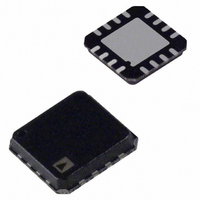
ADN2850BCP250-RL7 Analog Devices Inc, ADN2850BCP250-RL7 Datasheet - Page 8

ADN2850BCP250-RL7
Manufacturer Part Number
ADN2850BCP250-RL7
Description
IC DGTL RHEO DL 25K 9BIT16LFCSP
Manufacturer
Analog Devices Inc
Datasheet
1.ADN2850BCPZ250-RL7.pdf
(28 pages)
Specifications of ADN2850BCP250-RL7
Rohs Status
RoHS non-compliant
Taps
1024
Resistance (ohms)
250K
Number Of Circuits
2
Temperature Coefficient
35 ppm/°C Typical
Memory Type
Non-Volatile
Interface
4-Wire SPI Serial
Voltage - Supply
3 V ~ 5.5 V, ±2.25 V ~ 2.75 V
Operating Temperature
-40°C ~ 85°C
Mounting Type
Surface Mount
Package / Case
16-LFCSP
Resistance In Ohms
250K
For Use With
EVAL-ADN2850-25EBZ - BOARD EVALUATION FOR ADN2850-25
ADN2850
PIN CONFIGURATION AND FUNCTION DESCRIPTIONS
Table 4. Pin Function Descriptions
Pin No.
1
2
3
4
5
6
7
8
9
10
11
12
13
14
15
16
Mnemonic
CLK
SDI
SDO
GND
V
V1
W1
B1
B2
W2
V2
V
WP
PR
CS
RDY
SS
DD
Description
Serial Input Register Clock. Shifts in one bit at a time on positive clock edges.
Serial Data Input. Shifts in one bit at a time on positive clock CLK edges. MSB loads first.
Serial Data Output. Serves readback and daisy-chain functions. Command 9 and Command 10 activate the SDO
output for the readback function, delayed by 24 or 25 clock pulses, depending on the clock polarity before and
after the data-word (see Figure 2 and Figure 3). In other commands, the SDO shifts out the previously loaded SDI
bit pattern, delayed by 24 or 25 clock pulses depending on the clock polarity (see Figure 2 and Figure 3). This
previously shifted out SDI can be used for daisy-chaining multiple devices. Whenever SDO is used, a pull-up
resistor in the range of 1 kΩ to 10 kΩ is needed.
Ground Pin, Logic Ground Reference.
Negative Supply. Connect to 0 V for single-supply applications. If V
2 mA for 15 ms when storing data to EEMEM.
Log Output Voltage 1. Generates voltage from an internal diode configured transistor.
Wiper Terminal of RDAC1. ADDR (RDAC1) = 0x0.
Terminal B of RDAC1.
Terminal B of RDAC2.
Wiper terminal of RDAC2. ADDR (RDAC2) = 0x1.
Log Output Voltage 2. Generates voltage from an internal diode configured transistor.
Positive Power Supply.
Optional Write Protect. When active low, WP prevents any changes to the present contents, except PR strobe.
CMD_1 and COMD_8 refresh the RDAC register from EEMEM. Tie WP to V
Optional Hardware Override Preset. Refreshes the scratchpad register with current contents of the EEMEM
register. Factory default loads midscale 512
at the logic high transition. Tie PR to V
Serial Register Chip Select Active Low. Serial register operation takes place when CS returns to logic high.
Ready. Active high open-drain output. Identifies completion of Instruction 2, Instruction 3, Instruction 8,
Instruction 9, Instruction 10, and PR.
SDO
GND
CLK
V
SDI
W1
B1
V1
SS
1
4
5
2
3
6
7
8
Figure 4. Pin Configuration
Rev. C | Page 8 of 28
(Not to Scale)
ADN2850
DD
TOP VIEW
, if not used.
10
until EEMEM is loaded with a new value by the user. PR is activated
16
15
14
13
12
10
11
9
RDY
CS
PR
WP
V
V2
W2
B2
DD
SS
is used in dual supply, it must be able to sink
DD
, if not used.


