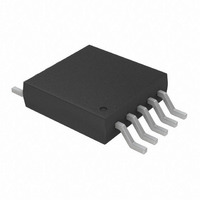
MCP4728-E/UN Microchip Technology, MCP4728-E/UN Datasheet - Page 40

MCP4728-E/UN
Manufacturer Part Number
MCP4728-E/UN
Description
IC DAC 12BIT W/I2C 10-MSOP
Manufacturer
Microchip Technology
Specifications of MCP4728-E/UN
Number Of Converters
4
Settling Time
6µs
Package / Case
10-MSOP, Micro10™, 10-uMAX, 10-uSOP
Number Of Bits
12
Data Interface
I²C
Voltage Supply Source
Single Supply
Operating Temperature
-40°C ~ 125°C
Mounting Type
Surface Mount
Number Of Dac Outputs
4
Resolution
12 bit
Interface Type
I2C
Supply Voltage (max)
5.5 V
Supply Voltage (min)
2.7 V
Maximum Operating Temperature
+ 125 C
Mounting Style
SMD/SMT
Minimum Operating Temperature
- 40 C
Supply Current
110 mA
Voltage Reference
2.048 V
Lead Free Status / RoHS Status
Lead free / RoHS Compliant
For Use With
MCP4728EV - BOARD EVAL 12BIT 4CH DAC MCP4728
Power Dissipation (max)
-
Lead Free Status / Rohs Status
Lead free / RoHS Compliant
Available stocks
Company
Part Number
Manufacturer
Quantity
Price
Part Number:
MCP4728-E/UN
Manufacturer:
MICROCHIP/微芯
Quantity:
20 000
MCP4728
FIGURE 5-9:
from Starting Channel to Channel D. The sequential input register starts with the "Starting Channel" and
ends at Channel D. For example, if DAC1:DAC0 = 00, then it starts with channel A and ends at channel D.
If DAC1:DAC0 = 01, then it starts with channel B and ends at Channel D. Note that this command can
send up to 10 bytes including the device addressing and command bytes. Any byte after the 10th byte is
ignored.
DS22187E-page 40
Command Type Bits:
Start
S
Note 1:
(C2 C1 C0 W1 W2)
0
Sequential Write
1
Command
1
2:
1
Device Addressing
0
The MCP4728 device starts writing EEPROM at the falling edge of the 4th byte’s ACK pulse.
V
If UDAC = 0 or LDAC Pin = 0: V
EEPROM Write:
0
OUT
1
1st byte
0
Update:
0 DAC1 DAC0 UDAC A V
A2 A1 A0
Sequential Write Command: Write DAC Input Registers and EEPROM Sequentially
Starting Channel
Sequential Write
C2=0
2nd Byte
Select
ACK (MCP4728)
R/W
0
C1=1
A
V
Repeat Bytes of the 3rd - 4th Bytes
for the Starting Channel + 1, ... until Channel D.
REF
OUT
C0=0
REF
PD1 PD0 Gx D11 D10 D9 D8 A D7 D6 D5 D4 D3 D2 D1 D0 A
is updated after the 4th byte’s ACK is issued.
PD1 PD0 Gx D11 D10 D9 D8 A D7 D6 D5 D4 D3 D2 D1 D0 A
W1=1
3rd Byte
3rd Byte
DAC Input Register of Starting Channel
DAC Input Register of Channel D
W0=0
(Last Channel)
ACK (MCP4728)
ACK (MCP4728)
© 2010 Microchip Technology Inc.
4th Byte
4th Byte
Notes 1 and 2
Note 1
Stop
P


