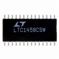
LTC1458CSW#PBF Linear Technology, LTC1458CSW#PBF Datasheet - Page 5

LTC1458CSW#PBF
Manufacturer Part Number
LTC1458CSW#PBF
Description
IC D/A CONV 12BIT R-R QUAD28SOIC
Manufacturer
Linear Technology
Datasheet
1.LTC1458CSWPBF.pdf
(12 pages)
Specifications of LTC1458CSW#PBF
Settling Time
14µs
Number Of Bits
12
Data Interface
Serial
Number Of Converters
4
Voltage Supply Source
Single Supply
Power Dissipation (max)
5.5mW
Operating Temperature
0°C ~ 70°C
Mounting Type
Surface Mount
Package / Case
28-SOIC (7.5mm Width)
Number Of Channels
4
Resolution
12b
Interface Type
Serial (3-Wire)
Single Supply Voltage (typ)
5V
Dual Supply Voltage (typ)
Not RequiredV
Power Supply Requirement
Single
Output Type
Voltage
Single Supply Voltage (min)
4.5V
Single Supply Voltage (max)
5.5V
Dual Supply Voltage (min)
Not RequiredV
Dual Supply Voltage (max)
Not RequiredV
Operating Temp Range
0C to 70C
Operating Temperature Classification
Commercial
Mounting
Surface Mount
Pin Count
28
Lead Free Status / RoHS Status
Lead free / RoHS Compliant
Available stocks
Company
Part Number
Manufacturer
Quantity
Price
PI FU CTIO S
TYPICAL PERFOR A CE CHARACTERISTICS
X1/X2 C, X1/X2 D,X1/X2 A, X1/X2 B (Pins 1, 14, 16, 27):
The Input Pin that Sets the Gain for DAC C/D/A/B. When
grounded the gain will be 2, i.e., output full-scale will be
2 • REFHI. When connected to V
output full-scale will be equal to REFHI.
V
Buffered DAC Outputs.
CS/LD (Pin 3): The Serial Interface Enable and Load
Control Input.
D
REFHI C, REFHI D, REFHI A, REFHI B,(Pins 5, 9, 20, 24):
The Inputs to the DAC Resistor Ladder for DAC C/D/A/B.
GND (Pins 6, 23): Ground.
OUT C
IN
4.110
4.105
4.100
4.095
4.090
4.085
4.080
U
(Pin 4): The Serial Data Input.
–55
LTC1458 Full-Scale Voltage vs
Temperature
, V
OUT D
–25
U
TEMPERATURE ( C)
, V
5
OUT A
U
35
, V
65
OUT B
W
95
(Pins 2, 13, 17, 26): The
OUT
1458 G06
U
125
the gain will be 1, i.e.,
–1
–2
–3
–4
–5
5
4
3
2
1
0
–55
LTC1458
Offset Voltage vs Temperature
–25
TEMPERATURE ( C)
5
35
REFLO C, REFLO D, REFLO A, REFLO B, (Pins 7, 8, 21,
22): The Bottom of the DAC Resistor Ladders for the
DACs. These can be used to offset zero-scale above
ground. REFLO should be connected to ground when no
offset is required.
D
Becomes Valid on the Rising Edge of the Serial Clock.
CLK (Pin 11): The Serial Interface Clock Input.
V
quires a 0.1 F bypass capacitor to ground.
REFOUT (Pin 19): The Output of the Internal Reference.
CLR (Pin 25): The Clear Pin. Clears all DACs to zero-scale
when pulled low.
CC
OUT
5.5V (LTC1458), 2.7V
(Pins 15, 28): The Positive Supply Input. 4.5V V
65
(Pin 10): The Output of the Shift Register which
95
1458 G07
125
950
940
930
920
910
900
890
880
870
860
850
LTC1458/LTC1458L
–55
LTC1458
Supply Current vs Temperature
V
–25
CC
TEMPERATURE ( C)
5.5V (LTC1458L). Re-
5
V
V
V
CC
CC
CC
= 4.5V
= 5.5V
= 5V
35
65
95
1458 G05
5
125
CC


