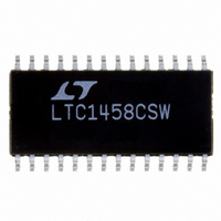
LTC1458CSW#PBF Linear Technology, LTC1458CSW#PBF Datasheet - Page 8

LTC1458CSW#PBF
Manufacturer Part Number
LTC1458CSW#PBF
Description
IC D/A CONV 12BIT R-R QUAD28SOIC
Manufacturer
Linear Technology
Datasheet
1.LTC1458CSWPBF.pdf
(12 pages)
Specifications of LTC1458CSW#PBF
Settling Time
14µs
Number Of Bits
12
Data Interface
Serial
Number Of Converters
4
Voltage Supply Source
Single Supply
Power Dissipation (max)
5.5mW
Operating Temperature
0°C ~ 70°C
Mounting Type
Surface Mount
Package / Case
28-SOIC (7.5mm Width)
Number Of Channels
4
Resolution
12b
Interface Type
Serial (3-Wire)
Single Supply Voltage (typ)
5V
Dual Supply Voltage (typ)
Not RequiredV
Power Supply Requirement
Single
Output Type
Voltage
Single Supply Voltage (min)
4.5V
Single Supply Voltage (max)
5.5V
Dual Supply Voltage (min)
Not RequiredV
Dual Supply Voltage (max)
Not RequiredV
Operating Temp Range
0C to 70C
Operating Temperature Classification
Commercial
Mounting
Surface Mount
Pin Count
28
Lead Free Status / RoHS Status
Lead free / RoHS Compliant
Available stocks
Company
Part Number
Manufacturer
Quantity
Price
DEFI ITIO S
Differential Nonlinearity (DNL): DNL is the difference
between the measured change and the ideal 1LSB change
between any two adjacent codes. The DNL error between
any two codes is calculated as follows:
OPERATIO
Serial Interface
The data on the D
on the rising edge of the clock. Data is loaded as one 48-bit
word, DAC A first, then DAC B, DAC C and DAC D. The MSB
is loaded first for each DAC. The DAC registers load the
data from the shift register when CS/LD is pulled high. The
CLK is disabled internally when CS/LD is high. Note: CLK
must be low before CS/LD is pulled low to avoid an extra
internal clock pulse.
The buffered output of the 48-bit shift register is available
on the D
Multiple LTC1458/LTC1458Ls may be daisy-chained to-
gether by connecting the D
chip, while the CLK and CS/LD signals remain common to
all chips in the daisy-chain. The serial data is clocked to all
of the chips, then the CS/LD signal is pulled high to update
all of them simultaneously.
LTC1458/LTC1458L
8
DNL
V
OUT
U
OUT
= ( V
= The measured voltage difference between
pin which swings from ground to V
two adjacent codes
U
OUT
U
IN
input is loaded into the shift register
– LSB)/LSB
OUT
pin to the D
IN
pin of the next
CC
.
Reference
The LTC1458L has an internal reference of 1.22V with a full
scale of 2.5V (gain of 2 configuration). The LTC1458
includes an internal 2.048V reference, making 1LSB equal
to 1mV (gain of 2 configuration). When the buffer gain is
2, the external reference must be less than V
capable of driving the 15k minimum DAC resistor ladder.
The external reference must always be less than
V
density at 1kHz is 300nV/ Hz.
Voltage Output
The rail-to-rail buffered output of the LTC1458 family can
source or sink 5mA when operating with a 5V supply over
the entire operating temperature range while pulling to
within 300mV of the positive supply voltage or ground.
The output swings to within a few millivolts of either
supply rail when unloaded and has an equivalent output
resistance of 40 when driving a load to the rails. The
output can drive 1000pF without going into oscillation.
The output voltage noise spectral density at 1kHz is
600nV/ Hz.
Digital Feedthrough: The glitch that appears at the analog
output caused by AC coupling from the digital inputs when
they change state. The area of the glitch is specified in
(nV)(sec).
CC
– 1.5V. The reference output voltage noise spectral
CC
/2 and be


