AD7302BNZ Analog Devices Inc, AD7302BNZ Datasheet - Page 2
AD7302BNZ
Manufacturer Part Number
AD7302BNZ
Description
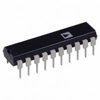
IC DAC 8BIT DUAL R-R 20-DIP
Manufacturer
Analog Devices Inc
Datasheet
1.AD7302BRUZ.pdf
(16 pages)
Specifications of AD7302BNZ
Data Interface
Parallel
Settling Time
1.2µs
Number Of Bits
8
Number Of Converters
2
Voltage Supply Source
Single Supply
Power Dissipation (max)
24.8mW
Operating Temperature
-40°C ~ 105°C
Mounting Type
Through Hole
Package / Case
20-DIP (0.300", 7.62mm)
Resolution (bits)
8bit
Sampling Rate
833kSPS
Input Channel Type
Parallel
Supply Voltage Range - Analog
2.7V To 5.5V
Supply Current
2.8mA
Digital Ic Case Style
DIP
Lead Free Status / RoHS Status
Lead free / RoHS Compliant
Available stocks
Company
Part Number
Manufacturer
Quantity
Price
Company:

Part Number:
AD7302BNZ
Manufacturer:
ADI
Quantity:
596


AD7302–SPECIFICATIONS
Parameter
STATIC PERFORMANCE
DAC REFERENCE INPUT
OUTPUT CHARACTERISTICS
LOGIC INPUTS
POWER REQUIREMENTS
NOTES
1
2
3
4
Specifications subject to change without notice.
Temperature ranges are as follows: B Version: –40 C to +105 C.
Relative Accuracy is calculated using a reduced code range of 15 to 245.
Gain error is specified between Codes 15 and 245. The actual error at Code 15 is typically 3 LSB.
Guaranteed by characterization at product release, not production tested.
Resolution
Relative Accuracy
Differential Nonlinearity
Full-Scale Error
Zero Code Error @ 25 C
Gain Error
Zero Code Temperature Coefficient
REFIN Input Range
REFIN Input Impedance
Output Voltage Range
Output Voltage Settling Time
Slew Rate
Digital to Analog Glitch Impulse
Digital Feedthrough
Digital Crosstalk
Analog Crosstalk
DC Output Impedance
Short Circuit Current
Power Supply Rejection Ratio
Input Current
V
V
V
V
Pin Capacitance
V
I
I
DD
DD
INL
INL
INH
INH
DD
V
V
@ 25 C
T
DD
DD
MIN
(Full Power-Down)
, Input Low Voltage
, Input Low Voltage
@ 25 C
@ T
@ 25 C
@ T
, Input High Voltage
, Input High Voltage
= 3.3 V
= 5.5 V
to T
MIN
MIN
3
MAX
to T
to T
MAX
MAX
4
B Versions
8
–0.75
3
100
1.0 to V
10
0 to V
2
7.5
1
0.2
0.2
40
14
0.0003
0.8
0.6
2.4
2.1
7
2.7/5.5
2.8
3
4.5
5
1
2
1
1
1
0.2
10
DD
DD
(V
to T
/2
DD
1
MAX
= +2.7 V to +5.5 V, Internal Reference; C
unless otherwise noted)
Units
Bits
LSB max
LSB max
LSB typ
LSB typ
% FSR typ
V min to max
M typ
V min to max
V/ s typ
nV-s typ
nV-s typ
nV-s typ
LSB typ
mA typ
%/% max
V max
V max
V min
V min
pF max
V min/max
mA max
mA max
mA max
mA max
V/ C typ
s max
A max
A max
A max
–2–
typ
Conditions/Comments
Note 2
Guaranteed Monotonic
All Zeroes Loaded to DAC Register
Typically 1.2 s
1 LSB Change Around Major Carry
V
V
V
V
Both DACs Active and Excluding Load Currents
V
Typically 2.3 mA
See Figures 6 and 7
V
Typically 2.8 mA
See Figures 6 and 7
V
See Figure 18
V
DD
DD
DD
DD
IH
IH
IH
DD
= V
= V
= V
= +5 V
= +3 V
= +5 V
= +3 V
= 10%
DD
DD
DD
and V
and V
and V
L
= 100 pF, R
IL
IL
IL
= GND
= GND
= GND
L
= 10 k
to V
DD
and GND;
REV. 0
Related parts for AD7302BNZ
Image
Part Number
Description
Manufacturer
Datasheet
Request
R

Part Number:
Description:
±1.7g Dual-Axis IMEMS Accelerometer Evaluation Board
Manufacturer:
Analog Devices Inc
Datasheet:

Part Number:
Description:
Inertial Sensor Evaluation System
Manufacturer:
Analog Devices Inc
Datasheet:
Part Number:
Description:
Manufacturer:
Analog Devices Inc
Datasheet:
Part Number:
Description:
Manufacturer:
Analog Devices Inc
Datasheet:
Part Number:
Description:
Manufacturer:
Analog Devices Inc
Datasheet:
Part Number:
Description:
Manufacturer:
Analog Devices Inc
Datasheet:
Part Number:
Description:
Manufacturer:
Analog Devices Inc
Datasheet:
Part Number:
Description:
Manufacturer:
Analog Devices Inc
Datasheet:
Part Number:
Description:
Manufacturer:
Analog Devices Inc
Datasheet:
Part Number:
Description:
Manufacturer:
Analog Devices Inc
Datasheet:
Part Number:
Description:
Manufacturer:
Analog Devices Inc
Datasheet:
Part Number:
Description:
Manufacturer:
Analog Devices Inc
Datasheet:
Part Number:
Description:
Manufacturer:
Analog Devices Inc
Datasheet: